PI6CV855-02LE Pericom Semiconductor, PI6CV855-02LE Datasheet
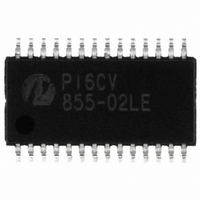
IC PLL CLOCK DVR SSTL_2 28-TSSOP

PI6CV855-02LE

Manufacturer Part Number
PI6CV855-02LE
Description
IC PLL CLOCK DVR SSTL_2 28-TSSOP
Manufacturer
Pericom Semiconductor
Type
PLL Clock Driverr
Datasheet

Specifications of PI6CV855-02LE

Pll
Yes with Bypass
Input
SSTL-2
Output
SSTL-2
Number Of Circuits
1
Ratio - Input:output
1:5
Differential - Input:output
Yes/Yes
Frequency - Max
200MHz
Divider/multiplier
No/No
Voltage - Supply
2.3 V ~ 2.7 V
Operating Temperature
0°C ~ 70°C
Mounting Type
Surface Mount
Package / Case
28-TSSOP
Frequency-max
200MHz
Lead Free Status / RoHS Status
Lead free / RoHS Compliant
1 2 3 4 5 6 7 8 9 0 1 2 3 4 5 6 7 8 9 0 1 2 3 4 5 6 7 8 9 0 1 2 1 2 3 4 5 6 7 8 9 0 1 2 3 4 5 6 7 8 9 0 1 2 3 4 5 6 7 8 9 0 1 2 1 2 3 4 5 6 7 8 9 0 1 2 3 4 5 6 7 8 9 0 1 2 3 4 5 6 7 8 9 0 1 2 1 2 3 4 5 6 7 8 9 0 1 2 3 4 5 6 7 8 9 0 1 2 3 4 5 6 7 8 9 0 1 2 1 2 3 4 5 6 7 8 9 0 1 2
1 2 3 4 5 6 7 8 9 0 1 2 3 4 5 6 7 8 9 0 1 2 3 4 5 6 7 8 9 0 1 2 1 2 3 4 5 6 7 8 9 0 1 2 3 4 5 6 7 8 9 0 1 2 3 4 5 6 7 8 9 0 1 2 1 2 3 4 5 6 7 8 9 0 1 2 3 4 5 6 7 8 9 0 1 2 3 4 5 6 7 8 9 0 1 2 1 2 3 4 5 6 7 8 9 0 1 2 3 4 5 6 7 8 9 0 1 2 3 4 5 6 7 8 9 0 1 2 1 2 3 4 5 6 7 8 9 0 1 2
Features
• PLL clock distribution optimized for SSTL_2
• Distributes one differential clock input pair to five differential
• Inputs (CLK,CLK) and (FBIN,FBIN): SSTL_2
• Outputs (Yx, Yx), (FBOUT, FBOUT): SSTL_2
• External feedback pins (FBIN,FBIN) are used to
• Operates at AV
• Packaging (Pb-free & Green available):
Block Diagram
clock output pairs.
synchronize the outputs to the input clocks.
and V
- 28-pin TSSOP (L28)
CLK
CLK
FBIN
FBIN
AV
DD
08-0298
DDQ
= 2.5V for differential output drivers
DD
Test Ciruit
= 2.5V for core circuit and internal PLL,
Logic
PLL
and
Y0
Y0
Y1
Y1
Y2
Y2
Y3
Y3
Y4
Y4
FBOUT
FBOUT
1
Description
The PI6CV855-02 PLL Clock Buffer is designed for 2.5 V
AV
device is a zero delay buffer that distributes a differential clock input
pair (CLK, CLK) to five differential pairs of clock outputs (Y[0:4],
Y[0:4]) and one differential pair feedback clock outputs (FBOUT,
FBOUT). The clock outputs are controlled by the input clocks (CLK,
CLK), the feedback clocks (FBIN,FBIN), and the Analog Power input
(AV
bypassed for test purposes.
The PI6CV855-02 is able to track Spread Spectrum Clocking to reduce
EMI.
Pin Configuration
DD
DD
operation and differential data input and output levels. The
). When the AV
200 MHz SSTL_2 PLL Clock Driver
V DDQ
AGND
V DDQ
AV DD
GND
GND
CLK
CLK
Y1
Y2
Y2
Y0
Y0
Y1
DD
is strapped low, the PLL is turned off and
1
2
3
4
5
6
7
8
9
10
11
12
13
14
28-Pin
L
28
27
26
25
24
23
22
21
20
19
18
17
16
15
PI6CV855-02
Y4
Y4
V DDQ
GND
FBOUT
FBOUT
V DDQ
FBIN
FBIN
GND
V DDQ
Y3
Y3
GND
PS8749B
DDQ
and 2.5V
11/13/08

Related parts for PI6CV855-02LE

PI6CV855-02LE Summary of contents

Page 1

... Y[0:4]) and one differential pair feedback clock outputs (FBOUT, FBOUT). The clock outputs are controlled by the input clocks (CLK, CLK), the feedback clocks (FBIN,FBIN), and the Analog Power input (AV ). When the bypassed for test purposes. The PI6CV855-02 is able to track Spread Spectrum Clocking to reduce EMI. Pin Configuration GND ...

Page 2

... Pinout Table Function Table 08-0298 200 MHz SSTL_2 PLL Clock Driver & PI6CV855- PS8749B 11/13/08 ...

Page 3

... Application clock frequency indicates a range over which the PLL meets all of the timing parameters. 08-0298 200 MHz SSTL_2 PLL Clock Driver – – – – ± PI6CV855- μ PS8749B 11/13/08 ...

Page 4

... DC Specifications Recommended Operating Conditions Electrical Characteristics Notes: 1. Driving memory chips with 120 Ohm termination resistor for each clock output pair at 134 MHz. 08-0298 – PI6CV855-02 200 MHz SSTL_2 PLL Clock Driver – – – – ± PS8749B ° μ 11/13/08 ...

Page 5

... The slew rate is determined from the IBIS model with test load shown in Figure 1. 3. The SSC requirements meet the Intel PC100 SDRAM Registered DIMM specification. 08-0298 200 MHz SSTL_2 PLL Clock Driver > 100 MHz (unless otherwise noted). CLK ± – – – – – – PI6CV855- PS8749B 11/13/08 ...

Page 6

... DDQ /2 –V DDQ /2 08-0298 =120 Figure 1. IBIS Model Output Load C=14pF –V DDQ /2 C=14pF –V DDQ /2 Figure 2. Output Load Test Circuit 6 PI6CV855-02 200 MHz SSTL_2 PLL Clock Driver DDR SDRAM DDR SDRAM SCOPE PS8749B 11/13/08 ...

Page 7

... CLK CLK FBIN FBIN CLK CLK FBIN FBIN Yx Yx Yx, FBOUT Yx, FBOUT 08-0298 Figure 3. Cycle-to-Cycle Jitter ∑ large number of samples) Figure 4. Static Phase Offset t sk(o) Figure 5. Output Skew 7 PI6CV855-02 200 MHz SSTL_2 PLL Clock Driver n PS8749B 11/13/08 ...

Page 8

... Outputs 08-0298 t cycle jit(per) cycle n Figure 6. Period Jitter t half period jit(hper) half period n Figure 7. Half-Period Jitter 80 sl(i), sl(o) sl(i), sl(o) Figure 8. Input and Output Slew Rates 8 PI6CV855-02 200 MHz SSTL_2 PLL Clock Driver n+1 half period 1 2 DDQ 80% 20% 0V PS8749B 11/13/08 ...

Page 9

... Package Outline Exclusive of Mold Flash and Metal Burr 2. Controlling dimentions in millimeters 3. Ref: JEDEC MO-153F/AE Ordering Information Ordering Code PI6CV855-02LE Notes: 1. Thermal characteristics can be found on the company web site at www.pericom.com/packaging/ Pericom Semiconductor Corporation • 1-800-435-2336 • www.pericom.com 08-0298 .169 4.3 .177 4.5 ...

Related keywords