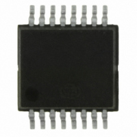
FS7140-02G-XTD ON Semiconductor, FS7140-02G-XTD Datasheet - Page 6

FS7140-02G-XTD
Manufacturer Part Number
FS7140-02G-XTD
Description
IC CLOCK GEN PLL PROGR 16-SSOP
Manufacturer
ON Semiconductor
Type
PLL Clock Generatorr
Datasheet
1.FS7145-01-XTP.pdf
(19 pages)
Specifications of FS7140-02G-XTD
Pll
Yes
Input
Crystal
Output
CMOS, PECL
Number Of Circuits
1
Ratio - Input:output
2:1
Differential - Input:output
No/Yes
Frequency - Max
400MHz
Divider/multiplier
Yes/No
Voltage - Supply
3 V ~ 3.6 V
Operating Temperature
0°C ~ 70°C
Mounting Type
Surface Mount
Package / Case
16-SSOP
Frequency-max
340MHz
Mounting Style
SMD/SMT
Max Input Freq
80 MHz
Max Output Freq
340 MHz
Number Of Outputs
1
Operating Supply Voltage
3.3 V
Operating Temperature Range
0 C to + 70 C
Supply Current
35 mA
Lead Free Status / RoHS Status
Lead free / RoHS Compliant
Other names
766-1029
Available stocks
Company
Part Number
Manufacturer
Quantity
Price
Company:
Part Number:
FS7140-02G-XTD
Manufacturer:
NXP
Quantity:
1 459
FS714x
Then:
R1 (from CLKP and CLKN output to VDD) =
R2 (from CLKP and CLKN output to GND) =
Rprgm (from VDD to IPRG pin) =
4.3 SYNC Circuitry
The FS7145 supports nearly instantaneous adjustment of the output CLK phase by the SYNC input. Either edge direction of SYNC
(positive-going or negative-going) is supported.
Example (positive-going SYNC selected): Upon the negative edge of SYNC input, a sequence begins to stop the CLK output. Upon the
positive edge, CLK resumes operation, synchronized to the phase of the SYNC input (plus a deterministic delay). This is performed by
control of the device post-divider. Phase resolution equal to ½ of the VCO period can be achieved (approximately down to 2ns).
5.0 I
device determines which mode is activated. A device that sends data onto the bus is defined as the transmitter, and a device receiving
data as the receiver.
I
V
5.1 Bus Conditions
Data transfer on the bus can only be initiated when the bus is not busy. During the data transfer, the data line (SDA) must remain stable
whenever the clock line (SCL) is high. Changes in the data line while the clock line is high will be interpreted by the device as a START
or STOP condition. The following bus conditions are defined by the I
5.1.1. Not Busy
Both the data (SDA) and clock (SCL) lines remain high to indicate the bus is not busy.
5.1.2. START Data Transfer
A high to low transition of the SDA line while the SCL input is high indicates a START condition. All commands to the device must be
preceded by a START condition.
2
C-bus logic levels noted herein are based on a percentage of the power supply (V
DD
, while a logic-zero corresponds to ground (V
2
C-bus Control Interface
R
75 * 3.3 / 2.4 =
103 ohms
R
75 * 3.3 / (3.3 - 2.4) =
275 ohms
26 * (V
26 * (3.3 * 75) / (2.4 - 1.6) / 3 =
2.68 Kohms
This device is a read/write slave device meeting all Philips I
controlled by a master device that generates the serial clock SCL, controls bus access and generates the START and STOP
conditions while the device works as a slave. Both master and slave can operate as a transmitter or receiver, but the master
LOAD
LOAD
* V
* V
DD
DD
DD
* R
/ V
/ (V
LOAD
HI
DD
) / (V
=
- V
HI
HI
) =
- V
LO
) / 3 =
SS
).
Rev. 5 | Page 6 of 19 | www.onsemi.com
2
C-bus protocol.
2
C-bus specifications except a "general call." The bus has to be
DD
). A logic-one corresponds to a nominal voltage of


