CY7B9920-2SC Cypress Semiconductor Corp, CY7B9920-2SC Datasheet

IC CLK BUFF SKEW 8OUT 24SOIC

CY7B9920-2SC

Manufacturer Part Number
CY7B9920-2SC
Description
IC CLK BUFF SKEW 8OUT 24SOIC
Manufacturer
Cypress Semiconductor Corp
Type
Fanout Distribution, Zero Delay Bufferr
Datasheet

Specifications of CY7B9920-2SC

Pll
Yes
Input
Clock
Output
CMOS
Number Of Circuits
1
Ratio - Input:output
1:8
Differential - Input:output
No/No
Frequency - Max
80MHz
Divider/multiplier
No/No
Voltage - Supply
4.5 V ~ 5.5 V
Operating Temperature
0°C ~ 70°C
Mounting Type
Surface Mount
Package / Case
24-SOIC (7.5mm Width)
Frequency-max
80MHz
Lead Free Status / RoHS Status
Contains lead / RoHS non-compliant
Other names
428-1377

Available stocks

Company
Part Number
Manufacturer
Quantity
Price
Part Number:
CY7B9920-2SC
Manufacturer:
CY
Quantity:
1
Features
Functional Description
The CY7B9910 and CY7B9920 Low Skew Clock Buffers offer
low-skew system clock distribution. These multiple-output
clock drivers optimize the timing of high-performance comput-
er systems. Eight individual drivers can each drive terminated
transmission lines with impedances as low as 50 while deliv-
ering minimal and specified output skews and full-swing logic
levels (CY7B9910 TTL or CY7B9920 CMOS).
The completely integrated PLL allows “zero delay” capability.
External divide capability, combined with the internal PLL, allows
distribution of a low-frequency clock that can be multiplied by virtu-
ally any factor at the clock destination. This facility minimizes clock
distribution difficulty while allowing maximum system clock speed
and flexibility.
Cypress Semiconductor Corporation
• All outputs skew <100 ps typical (250 max.)
• 15- to 80-MHz output operation
• Zero input to output delay
• 50% duty-cycle outputs
• Outputs drive 50
• Low operating current
• 24-pin SOIC package
• Jitter: <200 ps peak to peak, <25 ps RMS
• Compatible with Pentium™-based processors
Pentium is a trademark of Intel Corporation.
REF
Logic Block Diagram
FB
TEST
FS
7B9910–1
PHASE
FREQ
DET
FILTER
terminated lines
Controlled
Oscillator
Voltage
3901 North First Street
Q0
Q1
Q2
Q3
Q4
Q5
Q6
Q7
Block Diagram Description
Phase Frequency Detector and Filter
These two blocks accept inputs from the reference frequency
(REF) input and the feedback (FB) input and generate correc-
tion information to control the frequency of the Voltage-Con-
trolled Oscillator (VCO). These blocks, along with the VCO,
form a Phase-Locked Loop (PLL) that tracks the incoming
REF signal.
VCO
The VCO accepts analog control inputs from the PLL filter
block and generates a frequency. The operational range of the
VCO is determined by the FS control pin.
Test Mode
The TEST input is a three-level input. In normal system oper-
ation, this pin is connected to ground, allowing the
CY7B9910/CY7B9920 to operate as explained above. (For
testing purposes, any of the three-level inputs can have a re-
movable jumper to ground, or be tied LOW through a 100
resistor. This will allow an external tester to change the state of
these pins.)
If the TEST input is forced to its MID or HIGH state, the device
will operate with its internal phase-locked loop disconnected,
and input levels supplied to REF will directly control all outputs.
Relative output to output functions are the same as in normal
mode.
Pin Configuration
San Jose
V
V
V
V
GND
REF
CCQ
CCQ
CCN
CCN
NC
Q0
Q1
Q2
Q3
FS
November 1994 - Revised July 7, 1997
1
2
3
4
5
6
7
8
9
10
11
12
Top View
7B9910
7B9920
SOIC
CA 95134
13
14
24
23
22
21
20
19
18
17
16
15
Clock Buffer
Low Skew
CY7B9910
CY7B9920
GND
TEST
NC
GND
V
Q7
Q6
GND
Q5
Q4
V
FB
CCN
CCN
408-943-2600
7B9910–2

Related parts for CY7B9920-2SC

CY7B9920-2SC Summary of contents

Page 1

... Jitter: <200 ps peak to peak, <25 ps RMS • Compatible with Pentium™-based processors Functional Description The CY7B9910 and CY7B9920 Low Skew Clock Buffers offer low-skew system clock distribution. These multiple-output clock drivers optimize the timing of high-performance comput- er systems. Eight individual drivers can each drive terminated ...

Page 2

... Min. V Max. V – Min. V Max – 500 mV Min. V Max. 0 Max Max Max 0.4V –500 – CY7B9910 CY7B9920 Ambient Temperature + 10% – + 10% CY7B9920 Max. Min. Max. Unit V V –0.75 CC 0. – 1.35 0.8 –0.5 1. – – 500 mV 500 mV 500 mV 1.0 0.0 1 –500 ...

Page 3

... CC achieved. 2. Tested one output at a time, output shorted for less than one second, less than 10% duty cycle. Room temperature only. CY7B9920 outputs are not short circuit protected. 3. Total output current per output pair can be approximated by the following expression that includes device current plus load current: ...

Page 4

... TTL AC Test Load (CY7B9910 R1=100 R2=100 (Includes fixture and probe capacitance 7B9910–5 CMOS AC Test Load (CY7B9920) Switching Characteristics Over the Operating Range Parameter Description f Operating Clock NOM Frequency in MHz t REF Pulse Width HIGH RPWH t REF Pulse Width LOW RPWL ...

Page 5

... JR Notes: 7. Test measurement levels for the CY7B9910 are TTL levels (1.5V to 1.5V). Test measurement levels for the CY7B9920 are CMOS levels (V conditions assume signal transition times of 2ns or less and output loading as shown in the AC Test Loads and Waveforms unless otherwise specified. 8. Guaranteed by statistical correlation. Tested initially and after any design or process changes that may affect these parameters. ...

Page 6

... AC Timing Diagrams REF OTHER REF RPWL t RPWH t ODCV t ODCV t t SKEW SKEW 6 CY7B9910 CY7B9920 t JR 7B9910–8 ...

Page 7

... Cascaded clock buffers will accumulate low-frequency jitter because of the non-ideal filtering characteristics of the PLL filter not recommended that more than two clock buffers be connected in series. REF Figure 2. Board-to-Board Clock Distribution CY7B9910 CY7B9920 LOAD Z 0 LOAD Z 0 LOAD Z 0 LOAD Z 0 7B9910–9 LOAD ...

Page 8

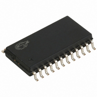
... CY7B9910–2SC CY7B9920–2SC 500 CY7B9910–5SC CY7B9910–5SI CY7B9920–5SC CY7B9920–5SI 750 CY7B9910–7SC CY7B9910–7SI CY7B9920–7SC CY7B9920–7SI Document #: 38–00437–B Package Diagram Package Name Package Type S13 24-Lead Small Outline IC S13 24-Lead Small Outline IC S13 24-Lead Small Outline IC ...

Related keywords