CY7B9920-2SC Cypress Semiconductor Corp, CY7B9920-2SC Datasheet - Page 3
CY7B9920-2SC
Manufacturer Part Number
CY7B9920-2SC
Description
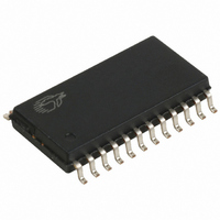
IC CLK BUFF SKEW 8OUT 24SOIC
Manufacturer
Cypress Semiconductor Corp
Type
Fanout Distribution, Zero Delay Bufferr
Datasheet
1.CY7B9920-5SC.pdf
(8 pages)
Specifications of CY7B9920-2SC
Pll
Yes
Input
Clock
Output
CMOS
Number Of Circuits
1
Ratio - Input:output
1:8
Differential - Input:output
No/No
Frequency - Max
80MHz
Divider/multiplier
No/No
Voltage - Supply
4.5 V ~ 5.5 V
Operating Temperature
0°C ~ 70°C
Mounting Type
Surface Mount
Package / Case
24-SOIC (7.5mm Width)
Frequency-max
80MHz
Lead Free Status / RoHS Status
Contains lead / RoHS non-compliant
Other names
428-1377
Available stocks
Company
Part Number
Manufacturer
Quantity
Price
Company:

Part Number:
CY7B9920-2SC
Manufacturer:
CY
Quantity:
1


Electrical Characteristics
Capacitance
I
I
I
I
PD
C
Notes:
Parameter
ILL
OS
CCQ
CCN
1.
2.
3.
4.
5.
6.
IN
Parameter
I
F = frequency in MHz
C = capacitive load in pF
Z = line impedance in ohms
N = number of loaded outputs; 0, 1, or 2
FC = F C
These inputs are normally wired to V
inputs at V
achieved.
Tested one output at a time, output shorted for less than one second, less than 10% duty cycle. Room temperature only. CY7B9920 outputs are not short
circuit protected.
Total output current per output pair can be approximated by the following expression that includes device current plus load current:
CY7B9910:
I
CY7B9920:
Where
Total power dissipation per output pair can be approximated by the following expression that includes device power dissipation plus power dissipation due to
the load circuit:
CY7B9910:
PD = [(22 + 0.61F) + [((1550 – 2.7F)/Z) + (.0125FC)]N] x 1.1
CY7B9920:
PD = [(19.25+ 0.94F) + [((700 + 6F)/Z) + (.017FC)]N] x 1.1
See note 3 for variable definition.
CMOS output buffer current and power dissipation specified at 50-MHz reference frequency.
Applies to REF and FB inputs only. Tested initially and after any design or process changes that may affect these parameters.
CCN
CCN
= [(3.5+ .17F) + [((1160 – 2.8F)/Z) + (.0025FC)]N] x 1.1
= [(4 + 0.11F) + [((835 – 3F)/Z) + (.0022FC)]N] x 1.1
CC
/2. If these inputs are switched, the function and timing of the outputs may glitch and the PLL may require an additional t
Input LOW Current
(Test, FS)
Output Short Circuit
Current
Operating Current Used by
Internal Circuitry
Output Buffer Current per
Output Pair
Power Dissipation per
Output Pair
[6]
Input Capacitance
[2]
Description
[3]
[4]
Description
CC
Over the Operating Range (continued)
, GND, or left unconnected (actual threshold voltages vary as a percentage of V
V
V
= GND (25 C only)
V
All Input
Selects Open
V
I
Input Selects Open, f
V
I
Input Selects Open, f
OUT
OUT
IN
CC
CCN
CCN
CCN
= GND
T
= Max., V
= 0 mA
= 0 mA
A
= V
Test Conditions
= V
= V
= 25 C, f = 1 MHz, V
CCQ
CCQ
CCQ
= Max.,
OUT
= Max.,
= Max.,
Test Conditions
3
MAX
MAX
Com’l
Mil/Ind
CC
= 5.0V
Min.
CY7B9910
Max.
–200
–250
CC
85
90
14
78
). Internal termination resistors hold unconnected
Max.
LOCK
10
Min.
time before all data sheet limits are
CY7B9920
CY7B9910
CY7B9920
104
Max.
–200
N/A
85
90
19
[5]
Unit
pF
Unit
mW
mA
mA
mA
A
Related parts for CY7B9920-2SC
Image
Part Number
Description
Manufacturer
Datasheet
Request
R

Part Number:
Description:
IC CLK BUFF SKEW 8OUT 24SOIC
Manufacturer:
Cypress Semiconductor Corp
Datasheet:

Part Number:
Description:
IC CLK BUFF SKEW 8OUT 24SOIC
Manufacturer:
Cypress Semiconductor Corp
Datasheet:

Part Number:
Description:
Phase Locked Loops (PLL) 5V,80MHz,8 CMOS Out non-programmable
Manufacturer:
Cypress Semiconductor Corp

Part Number:
Description:
CLOCK BUFFER CMOS OUT 32-PLCC
Manufacturer:
Cypress Semiconductor Corp
Datasheet:

Part Number:
Description:
CLOCK BUFFER CMOS OUT 32-PLCC
Manufacturer:
Cypress Semiconductor Corp
Datasheet:
Part Number:
Description:
Manufacturer:
Cypress Semiconductor Corp
Datasheet:
Part Number:
Description:
Manufacturer:
Cypress Semiconductor Corp
Datasheet:
Part Number:
Description:
IC CLK BUFF SKEW 8OUT 32PLCC
Manufacturer:
Cypress Semiconductor Corp
Datasheet:
Part Number:
Description:
IC,Eight Distributed-Output Clock Driver,LDCC,32PIN,PLASTIC
Manufacturer:
Cypress Semiconductor Corp
Datasheet:
Part Number:
Description:
Phase Locked Loops (PLL) 5V 80MHz 8 CMOS COM Programable
Manufacturer:
Cypress Semiconductor Corp
Part Number:
Description:
Manufacturer:
Cypress Semiconductor Corp
Datasheet: