CY28346ZXCT Cypress Semiconductor Corp, CY28346ZXCT Datasheet - Page 14
CY28346ZXCT
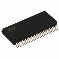
Manufacturer Part Number
CY28346ZXCT
Description
IC CLOCK SYNTHESIZER 56-TSSOP
Manufacturer
Cypress Semiconductor Corp
Type
Clock Synchronizer, Fanout Distribution, Spread Spectrum Clock Generatorr
Datasheet
1.CY28346OXC.pdf
(20 pages)
Specifications of CY28346ZXCT
Pll
Yes
Input
Clock, Crystal
Output
Clock
Number Of Circuits
1
Ratio - Input:output
5:17
Differential - Input:output
No/Yes
Frequency - Max
200MHz
Divider/multiplier
Yes/No
Voltage - Supply
3.135 V ~ 3.465 V
Operating Temperature
0°C ~ 70°C
Mounting Type
Surface Mount
Package / Case
56-TSSOP II
Frequency-max
200MHz
Lead Free Status / RoHS Status
Lead free / RoHS Compliant
Available stocks
Company
Part Number
Manufacturer
Quantity
Price

Part Number:
CY28346ZXCT
Manufacturer:
CYPRESS/赛普拉斯
Quantity:
20 000


Document #: 38-07331 Rev. *C
Maximum Ratings
Input Voltage Relative to V
Input Voltage Relative to V
Current Accuracy
DC Parameters
AC Parameters
Crystal
T
T
V
V
T
T
CPU at 0.7V Timing
T
T
T
Notes:
Iout
Iout
I
I
C
C
L
C
10. When Xin is driven from an external clock source.
12. All outputs loaded as perTable 9 below.
13. Probes are placed on the pins and measurements are acquired at 1.5V for 3.3V signals (see test and measurement set-up section of this data sheet).
14. Measured between 0.2V
15. This measurement is applicable with Spread ON or Spread OFF.
16. Measured at crossing point (Vx) or where subtraction of CLK–CLK# crosses 0V Measured from V
17. Measured from V
18. Determined as a fraction of 2*(Trise–Tfall)/ (Trise+Tfall).
19. Test load is Rta = 33.2Ω, Rd = 49.9Ω.
11. This is required for the duty cycle on the REF clock out to be as specified. The device will operate reliably with input duty cycles up to 30/70 but the REF clock
Parameter
DD
PD
5. Multiple Supplies: The Voltage on any input or I/O pin cannot exceed the power pin during power-up. Power supply sequencing is NOT required.
6. Inom refers to the expected current based on the configuration of the device.
7. All outputs loaded as per maximum capacitive load table.
8. Absolute value = ((Programmed CPU Iref) × (2)) + 10 mA.
9. This parameter is measured as an average over 1 µs duration, with a crystal center frequency of 14.31818 MHz.
DC
PERIOD
R
CCJ
DC
PERIOD
SKEW
Parameter
PIN
HIGH
LOW
IN
OUT
XTAL
Parameter
duty cycle will not be within data sheet specifications.
/ T
3.3V
3.3V
F
Dynamic Supply Current
Power-down Supply Current
Input Pin Capacitance
Output Pin Capacitance
Pin Inductance
Crystal Pin Capacitance
V
V
DD
DD
OL
X
X
X
X
X
X
CPUT and CPUC Duty
Cycle
CPUT and CPUC
Period
Any CPU to CPU Clock
Skew
IN
IN
IN
IN
IN
IN
= 0.175V to V
= nominal (3.30V)
= 3.30 ± 5%
(V
(V
Duty Cycle
period
HIGH Voltage
LOW Voltage
Rise and Fall Times
Cycle to Cycle Jitter
Conditions
DD
Description
DD
DD
Description
[6]
[5]
and 0.7V
= V
= V
SS
DDQ
:.............................. V
DDA
DDA
OH
or AV
DD
= 0.525V.
.
= 3.3V ±5%, TA = 0°C to +70°C)
= 3.3V ±5%, T
DD
: ............. V
M0 = 0 or 1 and Rr (see Table 1)
All combinations of M0 or 1 and Rr
(see Table 1)
0.7V
69.84
14.85
Min.
47.5
45
0
Measured from the X
66 MHz
DD
A
All frequencies at maximum values
= 0°C to +70°C)
DD
0.3V
SS
Max.
52.5
71.0
10.0
15.3
V
500
100
Configuration
55
+ 0.3V
DD
– 0.3V
DD
0.7V
69.84
Min.
47.5
9.85
PD# asserted
45
Conditions
0
100 MHz
DD
Storage Temperature: ................................ –65°C to + 150°C
Operating Temperature:.................................... 0°C to +85°C
Maximum Power Supply:................................................ 3.5V
IN
0.3V
or X
Max.
71.0
10.0
10.2
52.5
V
500
100
55
DD
DD
OUT
0.7V
69.84
pin to ground
Min.
47.5
7.35
OL
45
Nominal test load for given
configuration
Nominal test load for given
configuration
0
133 MHz
= 0.175V to V
DD
[7]
0.3V
Max.
71.0
52.5
10.0
7.65
V
500
100
55
DD
DD
Load
OH
0.7V
Min.
= 0.525V.
69.84
30
Min.
47.5
4.85
45
0
200 MHz
DD
Typ.
0.3V
36
Max.
52.5
71.0
10.0
V
500
100
5.1
55
DD
DD
Note 8
CY28346
Max.
–12%
Inom
Inom
280
Unit
Min.
–7%
Page 14 of 20
42
5
6
7
ns
ns
ps
ns
ps
%
%
V
V
9, 10, 11
12, 15,
15, 16,
15, 16,
12, 15,
Notes
13, 10
+ 12%
9, 12,
+ 7%
Max.
Inom
Inom
Unit
mA
mA
14
10
19
19
16
nH
pF
pF
pF
Related parts for CY28346ZXCT
Image
Part Number
Description
Manufacturer
Datasheet
Request
R

Part Number:
Description:
Manufacturer:
Cypress Semiconductor Corp
Datasheet:
Part Number:
Description:
Manufacturer:
Cypress Semiconductor Corp
Datasheet:
Part Number:
Description:
Manufacturer:
Cypress Semiconductor Corp
Datasheet:
Part Number:
Description:
Manufacturer:
Cypress Semiconductor Corp
Datasheet:
Part Number:
Description:
Manufacturer:
Cypress Semiconductor Corp
Datasheet: