CY28442ZXC Cypress Semiconductor Corp, CY28442ZXC Datasheet
CY28442ZXC
Specifications of CY28442ZXC
Available stocks


Related parts for CY28442ZXC

CY28442ZXC Summary of contents
Page 1
... Divider 96MSS PLL4 Divider FIXED VTTPWR_GD#/PD I2C SDATA Logic SCLK Cypress Semiconductor Corporation Document #: 38-07680 Rev. ** ADVANCE INFORMATION Clock Generator for Intel • 96/100 MHz Spreadable differential clock. • 33-MHz PCI clock • Low-voltage frequency select input 2 • support with readback capabilities • ...
Page 2
Pin Definitions Pin No. Name 1 VDD_REF PWR 3.3V power supply for outputs. 2 VSS_REF 33,32 CLKREQA#/SRCT6, I/O, PU 3.3V LVTTL input for enabling assigned SRC clock (active low) or 100 MHz CLKREQB#,SRCC6 7 VDD_PCI PWR 3.3V power supply for ...
Page 3
Pin Definitions (continued) Pin No. Name 48 VDDA2 PWR 3.3V power supply for PLL2. 49 XOUT O, SE 14.318-MHz crystal output. 50 XIN 51 VSSA2 52 REF1 53 FS_C_TEST_SEL/ REF0 54 CPU_STP# 55 PCI_STP# 56 PCI2/SEL_CLKREQ I/O, PD 3.3V-tolerant input ...
Page 4
Table 3. Block Read and Block Write Protocol Block Write Protocol Bit Description 1 Start 8:2 Slave address – 7 bits 9 Write 10 Acknowledge from slave 18:11 Command Code – 8 bits 19 Acknowledge from slave 27:20 Byte Count ...
Page 5
Control Registers Byte 0: Control Register 0 Bit @Pup Name 7 1 CPUT2_ITP/SRCT7 CPUC2_ITP/SRCC7 6 1 SRC[T/C SRC[T/C SRC[T/C SRC[T/C SRC[T/C SRC[T/C RESERVED Byte 1: Control Register 1 ...
Page 6
Byte 3: Control Register 3 Bit @Pup Name 7 0 SRC7 6 0 SRC6 5 0 SRC5 4 0 SRC4 3 0 SRC3 2 0 SRC2 1 0 SRC1 0 0 RESERVED Byte 4: Control Register 4 Bit @Pup Name ...
Page 7
Byte 5: Control Register 5 (continued) Bit @Pup Name 1 0 CPU[T/C CPU[T/C]0 Byte 6: Control Register 6 Bit @Pup Name 7 0 TEST_SEL 6 0 TEST_MODE 5 0 RESERVED 4 1 REF 3 1 PCI, PCIF and ...
Page 8
Byte 8: Control Register 8 (continued) Bit @Pup Name 3 0 RESERVED 2 1 CLKREQ CLKREQ RESERVED Byte 9: Control Register 9 Bit @Pup Name ...
Page 9
Byte 10: Control Register 10 (continued) Bit @Pup Name 2 0 CLKREQ CLKREQ CLKREQ#A The CY28442 requires a Parallel Resonance Crystal. Substi- tuting a series resonance crystal will cause the CY28442 to operate at the wrong ...
Page 10
Cs1 As mentioned previously, the capacitance on each side of the crystal is in series with the crystal. This mean the total capac- itance on each side of the crystal must be twice the specified load capacitance (CL). While the ...
Page 11
CLK_REQ[0:1]# Description The CLKREQ#[A:B] signals are active low input used for clean enabling and disabling selected SRC outputs. The outputs controlled by CLKREQ#[A:B] are determined by the settings in register byte 8. The CLKREQ# signal is a de-bounced signal CLKREQ#X ...
Page 12
PD CPUT, 133MHz CPUC, 133MHz SRCT 100MHz SRCC 100MHz USB, 48MHz DOT96T DOT96C PCI, 33 MHz REF Figure 4. Power-down Assertion Timing Waveform PD Deassertion The power-up latency is less than 1.8 ms. This is the time from the deassertion ...
Page 13
CPU_STP# CPUT CPUC CPU_STP# Deassertion The deassertion of the CPU_STP# signal will cause all CPU outputs that were stopped to resume normal operation in a synchronous manner. Synchronous manner meaning that no short or stretched clock pulses will be produce ...
Page 14
CPU_STOP# PD CPUT(Free Running) CPUC(Free Running) CPUT(Stoppable) CPUC(Stoppable) DOT96T DOT96C Figure 9. CPU_STP# = Tri-state, CPU_PD = Tri-state, DOT_PD = Tri-state PCI_STP# Assertion The PCI_STP# signal is an active LOW input used for synchronous stopping and starting the PCI outputs ...
Page 15
FS_A, FS_B,FS_C VTT_PW RGD# PW RGD_VRM 0.2-0.3mS VDD Clock Gen Clock State State 0 Off Clock Outputs Off Clock VCO VDD_A = 2.0V S0 Power Off Figure 13. Clock Generator Power-up/Run State Diagram Document #: 38-07680 Rev. ** ADVANCE INFORMATION ...
Page 16
Absolute Maximum Conditions Parameter Description V Core Supply Voltage DD V Analog Supply Voltage DD_A V Input Voltage IN T Temperature, Storage S T Temperature, Operating Ambient A T Temperature, Junction J Ø Dissipation, Junction to Case JC Ø Dissipation, ...
Page 17
AC Electrical Specifications Parameter Description Crystal T XIN Duty Cycle DC T XIN Period PERIOD XIN Rise and Fall Times XIN Cycle to Cycle Jitter CCJ L Long-term Accuracy ACC CPU at 0.7V T ...
Page 18
AC Electrical Specifications (continued) Parameter Description V Maximum Overshoot Voltage OVS V Minimum Undershoot Voltage UDS V Ring Back Voltage RB SRC T SRCT and SRCC Duty Cycle DC T 100-MHz SRCT and SRCC Period PERIOD T 100-MHz SRCT and ...
Page 19
AC Electrical Specifications (continued) Parameter Description DOT96T and DOT96C Rise and Fall R F Time T Rise/Fall Matching RFM ∆T Rise Time Variation R ∆T Fall Time Variation F V Voltage High HIGH V Voltage Low LOW ...
Page 20
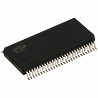
... Ω Ω Ω Figure 15. 0.7V Differential Load Configuration Figure 16. Single-ended Output Signals (for AC Parameters Measurement) Ordering Information Part Number Lead-free CY28442ZXC 56-pin TSSOP CY28442ZXCT 56-pin TSSOP – Tape and Reel Document #: 38-07680 Rev. ** ADVANCE INFORMATION Ω Ω Package Type CY28442 ...
Page 21
Package Diagrams 56-Lead Thin Shrunk Small Outline Package, Type mm) Z56 0.249[0.009 13.894[0.547] 14.097[0.555] 0.851[0.033] 0.500[0.020] 0.950[0.037] BSC Intel and Pentium are registered trademarks of Intel Corporation. All product and company names mentioned ...
Page 22
Document History Page Document Title: CY28442 Clock Generator for Intel Document Number: 38-07680 REV. ECN NO. Issue Date ** 237648 See ECN Document #: 38-07680 Rev. ** ADVANCE INFORMATION Alviso Chipset Orig. of Change Description of Change RGL New ...