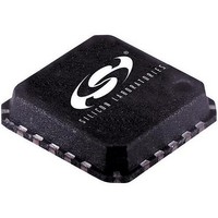
SI5310-GM Silicon Laboratories Inc, SI5310-GM Datasheet - Page 10

SI5310-GM
Manufacturer Part Number
SI5310-GM
Description
IC CLOCK MULT/REGENERATER 20MLP
Manufacturer
Silicon Laboratories Inc
Type
Clock Multiplierr
Datasheet
1.SI5310-BM.pdf
(26 pages)
Specifications of SI5310-GM
Number Of Circuits
1
Package / Case
20-VQFN Exposed Pad, 20-HVQFN, 20-SQFN, 20-DHVQFN
Pll
Yes with Bypass
Input
Clock
Output
CML
Ratio - Input:output
1:2
Differential - Input:output
Yes/Yes
Frequency - Max
668MHz
Divider/multiplier
Yes/Yes
Voltage - Supply
2.375 V ~ 2.625 V
Operating Temperature
-40°C ~ 85°C
Mounting Type
Surface Mount
Frequency-max
668MHz
Maximum Input Frequency
668 MHz
Minimum Input Frequency
9.375 MHz
Output Frequency Range
150 MHz to 668 MHz
Supply Voltage (max)
2.625 V
Supply Voltage (min)
2.375 V
Maximum Operating Temperature
+ 85 C
Minimum Operating Temperature
- 40 C
Mounting Style
SMD/SMT
Operating Supply Voltage
2.5 V
Lead Free Status / RoHS Status
Lead free / RoHS Compliant
Other names
336-1292-5
Table 8. Thermal Characteristics
Si5310
Table 6. Minimum Jitter Tolerance in Nanoseconds* (MULTSEL = 1, MULTOUT = 150 to 167 MHz)
Table 7. Absolute Maximum Ratings
10
Parameter
Thermal Resistance Junction to Ambient
*Note: Measured using sinusoidal jitter at stated Test Condition frequency.
Table 5. Minimum Jitter Tolerance in Nanoseconds* (MULTSEL = 0, MULTOUT = 600 to 668 MHz)
*Note: Measured using sinusoidal jitter at stated Test Condition frequency.
Parameter
DC Supply Voltage
LVTTL Input Voltage
Differential Input Voltages
Maximum Current any output PIN
Operating Junction Temperature
Storage Temperature Range
ESD HBM Tolerance (100 pf, 1.5 kΩ)
CLKIN+, CLKIN–, REFCLK+, REFCLK–,
All other pins
Note: Permanent device damage may occur if the above Absolute Maximum Ratings are exceeded. Functional operation
Frequency (Hz)
Frequency (Hz)
should be restricted to the conditions as specified in the operational sections of this data sheet. Exposure to absolute
maximum rating conditions for extended periods may affect device reliability.
< 300
250K
< 300
> 1M
325K
> 1M
6.5K
25K
65K
9.375–10.438 MHz
37.5–41.75 MHz
Clock Input
Clock Input
25.0
66.7
1.6
1.6
0.3
6.4
1.2
1.2
1.2
Symbol
18.75–20.875 MHz
ϕ
75–83.5 MHz
JA
Clock Input
Clock Input
Symbol
T
V
T
V
V
Rev. 1.2
STG
—
—
DIG
JCT
DIF
DD
25.0
66.7
13.0
3.2
3.2
0.3
1.9
1.9
1.9
Test Condition
Still Air
–0.3 to (V
37.5–41.75 MHz
150–167 MHz
–0.5 to 2.8
–0.3 to 3.6
–55 to 150
–55 to 150
Clock Input
Clock Input
Value
±50
1.5
25.0
66.7
29.0
1
1.9
1.9
1.9
6.5
3.0
0.5
DD
+ 0.3)
Value
38
300–334 MHz
75–83.5 MHz
Clock Input
Clock Input
25.0
66.7
33.3
Unit
mA
4.8
2.6
1.9
3.2
0.5
°C
°C
kV
kV
16
V
V
V
°C/W
Unit


