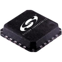
SI5310-GM Silicon Laboratories Inc, SI5310-GM Datasheet - Page 19

SI5310-GM
Manufacturer Part Number
SI5310-GM
Description
IC CLOCK MULT/REGENERATER 20MLP
Manufacturer
Silicon Laboratories Inc
Type
Clock Multiplierr
Datasheet
1.SI5310-BM.pdf
(26 pages)
Specifications of SI5310-GM
Number Of Circuits
1
Package / Case
20-VQFN Exposed Pad, 20-HVQFN, 20-SQFN, 20-DHVQFN
Pll
Yes with Bypass
Input
Clock
Output
CML
Ratio - Input:output
1:2
Differential - Input:output
Yes/Yes
Frequency - Max
668MHz
Divider/multiplier
Yes/Yes
Voltage - Supply
2.375 V ~ 2.625 V
Operating Temperature
-40°C ~ 85°C
Mounting Type
Surface Mount
Frequency-max
668MHz
Maximum Input Frequency
668 MHz
Minimum Input Frequency
9.375 MHz
Output Frequency Range
150 MHz to 668 MHz
Supply Voltage (max)
2.625 V
Supply Voltage (min)
2.375 V
Maximum Operating Temperature
+ 85 C
Minimum Operating Temperature
- 40 C
Mounting Style
SMD/SMT
Operating Supply Voltage
2.5 V
Lead Free Status / RoHS Status
Lead free / RoHS Compliant
Other names
336-1292-5
5. Pin Descriptions: Si5310
3, 8, 18, and
2, 7, 11, 14
GND Pad
Pin #
9, 10
4, 5
1
6
CLKIN+, CLKIN–
REFCLK+, REF-
Pin Name
REXT
CLK–
GND
VDD
LOL
Figure 11. Si5310 Pin Configuration
Table 11. Si5310 Pin Descriptions
I/O
O
I
I
REFCLK+
REFCLK–
REXT
GND
VDD
Signal Level
See Table 2
See Table 2
1
2
3
4
5
LVTTL
2.5 V
20
GND
6
Top View
19
Rev. 1.2
7
GND
Pad
18
8
17
9
External Bias Resistor.
This resistor is used by onboard circuitry to establish
bias currents within the device. This pin must be
connected to GND through a 10 kΩ (1%) resistor.
Supply Voltage.
Nominally 2.5 V.
Supply Ground.
Nominally 0.0 V. The GND pad found on the bottom
of the 20-pin micro leaded package (see Figure 12)
must be connected directly to supply ground.
Differential Reference Clock.
The reference clock sets the initial operating fre-
quency used by the onboard PLL for clock regenera-
tion and multiplication. Additionally, the reference
clock is used as a reference in generation of the LOL
output and to bound the frequency drift of MULTOUT
when CLKIN is not present.
Loss of Lock.
This output is driven high when a divided version of
the clock multiplier output deviates from the refer-
ence clock frequency by the amount specified in
Table 4 on page 8.
Differential Clock Input.
Differential input clock from which MULTOUT is
derived.
10
16
15
14
13
12
11
PWRDN
VDD
CLKOUT+
CLKOUT–
VDD
Description
Si5310
19


