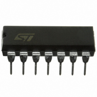
TS556CN STMicroelectronics, TS556CN Datasheet

TS556CN
Specifications of TS556CN
TS556CN
Available stocks
Related parts for TS556CN
TS556CN Summary of contents
Page 1
Features ■ Very low power consumption: 220 µA typ 180 µA typ ■ High maximum astable frequency 2.7 MHz ■ Pin-to-pin and functionally compatible with bipolar NE556 ■ ...
Page 2
Absolute maximum ratings and operating conditions 1 Absolute maximum ratings and operating conditions Table 1. Absolute maximum ratings Symbol V Supply voltage CC I Output current OUT Thermal resistance junction to ambient R thja Thermal resistance junction to case R ...
Page 3
TS556 2 Schematic diagram Figure 1. Schematic diagram (1/2 TS556) Schematic diagram 3/19 ...
Page 4
Schematic diagram Figure 2. Block diagram Table 3. Functions table Reset Low High High High LOW: level voltage ≤ minimum voltage specified Note: HIGH: level voltage ≥ maximum voltage specified x: irrelevant. 4/ Reset ...
Page 5
TS556 3 Electrical characteristics Table 4. Static electrical characteristics V CC Symbol Supply current (no load, high and low states ≤ min. Control voltage level V CL ≤ min. Discharge saturation voltage (I V ...
Page 6
Electrical characteristics Table 5. Static electrical characteristics V CC Symbol Supply current (no load, high and low states ≤ min amb Control voltage level V CL ≤ min amb Discharge saturation voltage (I V ...
Page 7
TS556 Table 6. Dynamic electrical characteristics V CC Symbol Timing accuracy (monostable kΩ 0.1 µF Timing shift with supply voltage variations (Monostable kΩ 0.1 µF, V Timing shift ...
Page 8
Electrical characteristics Table 7. Static electrical characteristics V CC Symbol Supply current (no load, high and low states ≤ min. Control voltage level V CL ≤ min. Discharge saturation voltage (I V DIS ≤ ...
Page 9
TS556 Table 8. Dynamic electrical characteristics V CC Symbol Timing accuracy (monostable kΩ 0.1 µF Timing shift with supply voltage variations (monostable kΩ 0.1 µF, V Timing shift ...
Page 10
Electrical characteristics Table 9. Static electrical characteristics V CC Symbol Supply current (no load, high and low states ≤ min. Control voltage level V CL ≤ min. Discharge saturation voltage (I V DIS ≤ ...
Page 11
TS556 Figure 3. Supply current (per timer) versus supply voltage 300 200 100 SUPPLY VOLTAGE, V (V) CC Electrical characteristics 11/19 ...
Page 12
Application information 4 Application information 4.1 Monostable operation In the monostable mode, the timer operates like a one-shot generator. Referring to figure 2, the external capacitor is initially held discharged by a transistor inside the timer, as shown in Figure ...
Page 13
TS556 4.2 Astable operation When the circuit is connected as shown in and runs as a multivibrator. The external capacitor charges through R discharges through R two resistors. In the astable mode of operation, C charges and discharges between 1/3 ...
Page 14
... These packages have a lead-free second level interconnect. The category of second level interconnect is marked on the package and on the inner box label, in compliance with JEDEC Standard JESD97. The maximum ratings related to soldering conditions are also marked on the inner box label. ECOPACK is an STMicroelectronics trademark. ECOPACK specifications are available at: www.st.com. 14/19 ...
Page 15
TS556 5.1 DIP14 package information Figure 8. DIP14 package mechanical drawing Table 11. DIP14 package mechanical data Ref Note: D and E1 dimensions do not include ...
Page 16
Package information 5.2 SO-14 package information Figure 9. SO-14 package mechanical drawing Table 12. SO-14 package mechanical data Ref ddd Note: D and F dimensions do not include ...
Page 17
... Package DIP14 0°C, +70°C SO-14 DIP14 -40°C, +125°C SO-14 DIP14 -55°C, +125°C SO-14 Ordering information Packaging Marking Tube TS556CN Tube or 556C Tape & reel Tube TS556IN Tube or 556I Tape & reel Tube TS556MN Tube or 556M Tape & reel 17/19 ...
Page 18
Revision history 7 Revision history Table 14. Document revision history Date 01-Feb-2003 28-Oct-2008 18/19 Revision 1 Initial release. Document reformatted. Added output current, ESD and thermal resistance values in Table 1: Absolute maximum 2 Added output current values in Updated ...
Page 19
... TS556 Information in this document is provided solely in connection with ST products. STMicroelectronics NV and its subsidiaries (“ST”) reserve the right to make changes, corrections, modifications or improvements, to this document, and the products and services described herein at any time, without notice. All ST products are sold pursuant to ST’s terms and conditions of sale. ...


