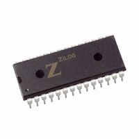
Z84C3006PEG Zilog, Z84C3006PEG Datasheet - Page 33

Z84C3006PEG
Manufacturer Part Number
Z84C3006PEG
Description
IC 6MHZ Z80 CMOS CTC 28-PDIP
Manufacturer
Zilog
Type
Counter/Timer Circuit (CTC)r
Series
Z80r
Specifications of Z84C3006PEG
Frequency
6MHz
Voltage - Supply
4.5 V ~ 5.5 V
Current - Supply
8mA
Operating Temperature
-40°C ~ 100°C
Package / Case
28-DIP (0.600", 15.24mm)
Processor Series
Z84C3xx
Core
Z80
Data Bus Width
8 bit
Maximum Clock Frequency
6 MHz
Operating Supply Voltage
0 V to 5 V
Maximum Operating Temperature
+ 100 C
Mounting Style
Through Hole
Minimum Operating Temperature
- 40 C
Filter Terminals
SMD
Ic Generic Number
84C30
Operating Temperature Min
-40°C
Operating Temperature Max
100°C
Clock Frequency
6MHz
Rohs Compliant
Yes
Cpu Speed
6MHz
Digital Ic Case Style
DIP
No. Of Pins
28
Supply Voltage Range
5V
Operating Temperature Range
-40°C To +100°C
Lead Free Status / RoHS Status
Lead free / RoHS Compliant
Count
-
Lead Free Status / Rohs Status
Details
Other names
269-3910
Z84C3006PEG
Z84C3006PEG
Available stocks
Company
Part Number
Manufacturer
Quantity
Price
Company:
Part Number:
Z84C3006PEG
Manufacturer:
ZILOG
Quantity:
1 980
Company:
Part Number:
Z84C3006PEG
Manufacturer:
Zilog
Quantity:
1 722
Company:
Part Number:
Z84C3006PEG
Manufacturer:
ZILOG
Quantity:
1 980
Company:
Part Number:
Z84C3006PEG
Manufacturer:
WSI
Quantity:
4 970
Part Number:
Z84C3006PEG
Manufacturer:
ZILOG
Quantity:
20 000
- Current page: 33 of 308
- Download datasheet (2Mb)
UM008005-0205
A
D
15
7
MREQ
RFSH
WAIT
— D
— A
CLK
RD
M1
Memory Read Or Write
0
0
segments from being gated onto the data bus. The MREQ signal during
refresh time should be used to perform a refresh read of all memory
elements. The refresh signal can not be used by itself because the refresh
address is only guaranteed to be stable during MREQ time.
Figure 5.
Figure 6 illustrates the timing of memory read or write cycles other than an
Op Code fetch cycle. These cycles are generally three clock periods long
unless wait states are requested by the memory through the WAIT signal.
The MREQ signal and the RD signal are used the same as in the fetch cycle.
In a memory write cycle, the MREQ also becomes active when the address
bus is stable so that it can be used directly as a chip enable for dynamic
memories. The WR line is active when data on the data bus is stable so that
T
PC
1
Instruction Op Code Fetch
T
2
M1 Cycle
IN
T
3
Refresh Address
T
4
T
User’s Manual
1
Z80 CPU
Overview
13
Related parts for Z84C3006PEG
Image
Part Number
Description
Manufacturer
Datasheet
Request
R

Part Number:
Description:
Communication Controllers, ZILOG INTELLIGENT PERIPHERAL CONTROLLER (ZIP)
Manufacturer:
Zilog, Inc.
Datasheet:

Part Number:
Description:
KIT DEV FOR Z8 ENCORE 16K TO 64K
Manufacturer:
Zilog
Datasheet:

Part Number:
Description:
KIT DEV Z8 ENCORE XP 28-PIN
Manufacturer:
Zilog
Datasheet:

Part Number:
Description:
DEV KIT FOR Z8 ENCORE 8K/4K
Manufacturer:
Zilog
Datasheet:

Part Number:
Description:
KIT DEV Z8 ENCORE XP 28-PIN
Manufacturer:
Zilog
Datasheet:

Part Number:
Description:
DEV KIT FOR Z8 ENCORE 4K TO 8K
Manufacturer:
Zilog
Datasheet:

Part Number:
Description:
CMOS Z8 microcontroller. ROM 16 Kbytes, RAM 256 bytes, speed 16 MHz, 32 lines I/O, 3.0V to 5.5V
Manufacturer:
Zilog, Inc.
Datasheet:

Part Number:
Description:
Low-cost microcontroller. 512 bytes ROM, 61 bytes RAM, 8 MHz
Manufacturer:
Zilog, Inc.
Datasheet:

Part Number:
Description:
Z8 4K OTP Microcontroller
Manufacturer:
Zilog, Inc.
Datasheet:

Part Number:
Description:
CMOS SUPER8 ROMLESS MCU
Manufacturer:
Zilog, Inc.
Datasheet:

Part Number:
Description:
SL1866 CMOSZ8 OTP Microcontroller
Manufacturer:
Zilog, Inc.
Datasheet:

Part Number:
Description:
SL1866 CMOSZ8 OTP Microcontroller
Manufacturer:
Zilog, Inc.
Datasheet:

Part Number:
Description:
OTP (KB) = 1, RAM = 125, Speed = 12, I/O = 14, 8-bit Timers = 2, Comm Interfaces Other Features = Por, LV Protect, Voltage = 4.5-5.5V
Manufacturer:
Zilog, Inc.
Datasheet:

Part Number:
Description:
Manufacturer:
Zilog, Inc.
Datasheet:


