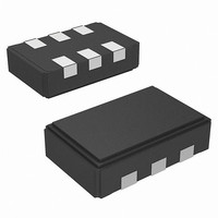
CY2X013FLXIT Cypress Semiconductor Corp, CY2X013FLXIT Datasheet - Page 4

CY2X013FLXIT
Manufacturer Part Number
CY2X013FLXIT
Description
IC XTAL OSC FIELD PROGR 6CLCC
Manufacturer
Cypress Semiconductor Corp
Specifications of CY2X013FLXIT
Pll
Yes
Input
Crystal
Output
LVDS
Number Of Circuits
1
Ratio - Input:output
1:1
Differential - Input:output
No/Yes
Frequency - Max
690MHz
Divider/multiplier
Yes/No
Voltage - Supply
*
Operating Temperature
*
Mounting Type
Surface Mount
Package / Case
6-CLCC
Frequency
*
Count
*
Operating Supply Voltage (typ)
2.5/3.3
Output Level
LVDS
Symmetry Max
60%
Operating Temp Range
-40C to 85C
Screening Level
Industrial
Lead Free Status / RoHS Status
Lead free / RoHS Compliant
AC Electrical Characteristics
The following table lists the AC electrical specifications for this device.
Switching Waveforms
Document Number: 001-10261 Rev. *E
F
FSC
FSI
AG
T
T
T
T
T
T
Notes
OHZ
OE
OUT
DC
R
LOCK
Jitter(φ)
4. Not 100% tested, guaranteed by design and characterization.
5. This parameter is specified in the CyClockWizard software.
6. Frequency stability is the maximum variation in frequency from F
7. Typical phase noise specs for factory programmed devices are listed in the
Parameter
, T
F
Output frequency
Frequency stability, commercial
devices
Frequency stability, industrial
devices
Aging, 10 years
Output duty cycle
Output rise and fall time
Output disable time
Output enable time
Startup time
RMS phase jitter (random)
[6]
[6]
Description
[5]
CLK#
CLK
Figure 2. Output Voltage Swing
Figure 3. Output Offset Voltage
V
V
F > 450 MHz, measured at zero crossing
outputs (asynchronous)
a valid frequency (asynchronous)
measured from the time
V
F
Pre-defined factory configurations
F <= 450 MHz, measured at zero crossing
20% and 80% of full output swing
Time from falling edge on OE to stopped
Time from rising edge on OE to outputs at
Time for CLK to reach valid frequency
CLK#
CLK
OUT
DD
DD
DD
0
= min to max, T
= min to max, T
= V
. It includes initial accuracy, and variation from temperature and supply voltage.
= 106.25 MHz (12 kHz to 20 MHz)
DD
ΔV
(min) or from PD# rising edge
Standard and Application-Specific Factory Configurations
OD
V
Condition
= V
OD1
[4]
OD1
A
A
50 Ω
50 Ω
= 0 °C to 70 °C
= –40 °C to 85 °C
- V
OD2
V
V
OS
OD2
[7]
Min
50
45
40
–
–
–
–
–
–
–
–
See Note 7
0.35
Typ
50
50
–
–
–
–
–
–
–
1
table on page 2.
Max
690
±35
±55
±15
100
120
CY2X013
1.0
55
60
5
–
Page 4 of 9
MHz
Unit
ppm
ppm
ppm
ms
ns
ns
ns
ps
ps
%
%
[+] Feedback


