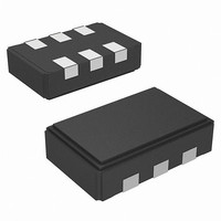
CY2X013FLXIT Cypress Semiconductor Corp, CY2X013FLXIT Datasheet - Page 2

CY2X013FLXIT
Manufacturer Part Number
CY2X013FLXIT
Description
IC XTAL OSC FIELD PROGR 6CLCC
Manufacturer
Cypress Semiconductor Corp
Specifications of CY2X013FLXIT
Pll
Yes
Input
Crystal
Output
LVDS
Number Of Circuits
1
Ratio - Input:output
1:1
Differential - Input:output
No/Yes
Frequency - Max
690MHz
Divider/multiplier
Yes/No
Voltage - Supply
*
Operating Temperature
*
Mounting Type
Surface Mount
Package / Case
6-CLCC
Frequency
*
Count
*
Operating Supply Voltage (typ)
2.5/3.3
Output Level
LVDS
Symmetry Max
60%
Operating Temp Range
-40C to 85C
Screening Level
Industrial
Lead Free Status / RoHS Status
Lead free / RoHS Compliant
Pinouts
Table 1. Pin Definitions - 6-Pin Ceramic LCC
Standard and Application-Specific Factory Configurations
Document Number: 001-10261 Rev. *G
1
4, 5
2
6
3
CY2X013LXI062T
CY2X013LXI100T
CY2X013LXI122T
CY2X013LXI125T
CY2X013LXI156T
CY2X013LXI200T
Pin
Part Number
CLK, CLK#
OE/PD#
Name
DNU
V
V
DD
SS
LVDS output Differential output clock
CMOS input Output enable pin: Active HIGH. If OE = 1, CLK is enabled.
I/O Type
Power
Power
–
Output Frequency
100.00 MHz
122.88 MHz
125.00 MHz
156.25 MHz
200.00 MHz
62.50 MHz
Power-down pin: Active LOW. If PD# = 0, the device is powered down and the clock is disabled.
The functionality of this pin is programmable
Do not use: DNU pins are electrically connected, but perform no function
Supply voltage: 2.5 V or 3.3 V
Ground
Figure 1. Pin Diagram – 6-Pin Ceramic LCC
OE/PD#
Pin 1 Function
DNU
V
SS
OE
OE
OE
OE
OE
OE
1
2
3
6
5 CLK#
4
V
CLK
DD
Description
1.875 MHz to 20 MHz
1.875 MHz to 20 MHz
1.875 MHz to 20 MHz
900 kHz to 7.5 MHz
637 kHz to 10 MHz
12 kHz to 20 MHz
12 kHz to 20 MHz
12 kHz to 20 MHz
12 kHz to 20 MHz
Offset Range
RMS Phase Jitter (Random)
Jitter (Typical)
CY2X013
0.36 ps
0.96 ps
0.52 ps
0.39 ps
0.81 ps
0.34 ps
0.84 ps
0.31 ps
0.74 ps
Page 2 of 10
[+] Feedback


