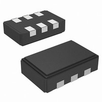
CY2XF24FLXCT Cypress Semiconductor Corp, CY2XF24FLXCT Datasheet - Page 3

CY2XF24FLXCT
Manufacturer Part Number
CY2XF24FLXCT
Description
IC XTAL OSC LVPECL I2C 6CLCC
Manufacturer
Cypress Semiconductor Corp
Datasheet
1.CY2XF24FLXCT.pdf
(15 pages)
Specifications of CY2XF24FLXCT
Package / Case
6-CLCC
Pll
Yes
Input
Crystal
Output
LVPECL
Number Of Circuits
1
Ratio - Input:output
1:1
Differential - Input:output
No/Yes
Frequency - Max
690MHz
Divider/multiplier
Yes/No
Voltage - Supply
*
Operating Temperature
*
Mounting Type
Surface Mount
Frequency
*
Count
*
Operating Supply Voltage (typ)
2.5/3.3
Output Level
LVPECL
Symmetry Max
60%
Operating Temp Range
0C to 70C
Screening Level
Commercial
Lead Free Status / RoHS Status
Lead free / RoHS Compliant
Standard and Application-Specific Factory Configurations
Functional Description
The CY2XF24 is a PLL-based high-performance clock
generator. It uses an internal crystal oscillator as a reference,
and outputs one differential LVPECL clock. It has an I
serial interface
The CY2XF24 comes configured for four different frequencies.
At power-on, the four configurations are transparently loaded
into an internal volatile memory which, in turn, controls the PLL.
You can switch between the four frequencies through the I
bus. You can also configure the CY2XF24 with new output
frequencies by shifting new data into the internal memory.
Frequency margining is a common application for this feature.
One frequency is used for the standard operating mode of the
device, while additional frequencies are available for margin
testing, either during product development or in-system
manufacturing test.
Note that all configuration changes made using I
temporary and are lost when power is removed from the device.
At power-on, the device returns to its original state.
The configuration for a particular frequency is stored in a 6-byte
block of memory, known as a word. The CY2XF24 has four such
words, labeled ‘Frequency Word 0’ through ‘Frequency Word 3’.
An additional register byte contains a 2-bit field, which selects
one of the four frequency words. By writing to this Select Byte,
you can switch back and forth between the four programmed
frequencies. The select byte can be configured to select any of
the four frequency words at power on.
When changing the output frequency, the frequency transition is
not guaranteed to be smooth. There can be frequency
excursions beyond the start frequency and the new frequency.
Glitches and runt pulses are possible, and time must be allowed
for the PLL to relock.
If more than four frequencies are needed, the I
used to change any of the four frequency words. When writing
frequency words through I
currently selected word. Instead, write one of the three
unselected words before changing the select byte to select that
new word.
Figure 2
selected.
Document Number: 001-53146 Rev. *D
CY2XF24LXI625T
Note
1. The serial interface is I
to V
Part Number
DD
shows how the frequency words are arranged and
, setup time, and output hold time.
[1]
, which is used to change the output frequency.
2
C Bus compliant, with the following exceptions: SDA input leakage current, SDA input capacitance, SDA and SCLK are clamped
2
625.00 MHz (default)
Output Frequency
C, you should not change the
78.125 MHz
156.25 MHz
312.50 MHz
2
C Bus can be
PRELIMINARY
Frequency Word
2
2
C are
C bus
2
C
0
1
2
3
Figure 2. Frequency Words
Configuration Software
Cypress provides
to create data values for shifting into the frequency words. This
software is required because the algorithm is too complicated to
be described here.
The user specifies the output frequency. The software then
calculates the bit stream for up to four frequency words, as
outlined by the register addresses for each word seen in
Figure
Programming Description
The CY2XF24 is a programmable device. Before being used in
an application, it must be programmed with the output
frequencies and other variables described in
Variables
each with its own programming flow. They are described in the
following section.
Field-Programmable CY2XF24F
Field programmable devices are shipped unprogrammed and
must be programmed before being installed on a printed circuit
board (PCB). Customers use
specify the device configuration and generate a joint electron
devices
programming file. Programming of samples and prototype
quantities is available using the CyClockWizard software along
with a
Kit
added distribution partners also provide programming services.
Field programmable devices are designated with an ‘F’ in the
part number. They are intended for quick prototyping and
inventory reduction. The software and programmer kit hardware
can be downloaded from
hyperlinks above.
10h – 15h
16h – 1Bh
1Ch – 21h
22h – 27h
Register
Address
with a
40h
CY3675-CLKMAKER1 CyClockMaker Clock Programmer
2.
on page 4. Two different device types are available,
Select Byte
engineering
CY3675-LCC6A socket
1.875 MHz to 20 MHz
1.875 MHz to 20 MHz
1.875 MHz to 20 MHz
1.875 MHz to 20 MHz
Offset Range
Frequency Word 0
Frequency Word 1
Frequency Word 2
Frequency Word 3
CyClockWizard™
RMS Phase Jitter (Random)
council
www.cypress.com
Bits [1:0]
CyClockWizard™
software that enables users
adapter. Cypress’s value
(JEDEC - extension .jed)
00
01
10
11
Sel
Jitter (Typical)
CY2XF24
by clicking the
0.37 ps
0.31 ps
0.29 ps
0.31 ps
Control
Programming
Page 3 of 15
Software to
PLL
[+] Feedback


