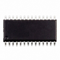
M48T08Y-10MH1F STMicroelectronics, M48T08Y-10MH1F Datasheet - Page 10

M48T08Y-10MH1F
Manufacturer Part Number
M48T08Y-10MH1F
Description
IC TIMEKPR SRAM 64KBIT 5V 28SOIC
Manufacturer
STMicroelectronics
Series
Timekeeper®r
Type
Clock/Calendar/NVSRAMr
Datasheet
1.M48T08Y-10MH1F.pdf
(31 pages)
Specifications of M48T08Y-10MH1F
Memory Size
64K (8K x 8)
Time Format
HH:MM:SS (24 hr)
Date Format
YY-MM-DD-dd
Interface
Parallel
Voltage - Supply
4.5 V ~ 5.5 V
Operating Temperature
0°C ~ 70°C
Mounting Type
Surface Mount
Package / Case
28-SOIC, 28-SOH (8.48mm Width)
Bus Type
Parallel
User Ram
8KB
Operating Supply Voltage (typ)
5V
Package Type
SOH
Operating Supply Voltage (max)
5.5V
Operating Supply Voltage (min)
4.5V
Operating Temperature Classification
Commercial
Operating Temperature (max)
70C
Operating Temperature (min)
0C
Pin Count
28
Mounting
Surface Mount
Lead Free Status / RoHS Status
Lead free / RoHS Compliant
Other names
497-4710-2
Available stocks
Company
Part Number
Manufacturer
Quantity
Price
Operation modes
Table 3.
Note:
2.2
10/31
Symbol
t
t
t
t
t
t
t
t
t
t
t
E2HQV
E2HQX
E1HQZ
t
E1LQV
E1LQX
E2LQZ
GHQZ
AVQV
GLQV
GLQX
AXQX
AVAV
READ mode AC characteristics
Valid for ambient operating temperature: T
(except where noted).
WRITE mode
The M48T08/18/08Y is in the WRITE mode whenever W, E1, and E2 are active. The start of
a WRITE is referenced from the latter occurring falling edge of W or E1, or the rising edge of
E2. A WRITE is terminated by the earlier rising edge of W or E1, or the falling edge of E2.
The addresses must be held valid throughout the cycle. E1 or W must return high or E2 low
for a minimum of t
initiation of another READ or WRITE cycle. Data-in must be valid t
WRITE and remain valid for t
avoid bus contention; however, if the output bus has been activated by a low on E1 and G
and a high on E2, a low on W will disable the outputs t
READ cycle time
Address valid to output valid
Chip enable 1 low to output valid
Chip enable 2 high to output valid
Output enable low to output valid
Chip enable 1 low to output transition
Chip enable 2 high to output transition
Output enable low to output transition
Chip enable 1 high to output Hi-Z
Chip enable 2 low to output Hi-Z
Output enable high to output Hi-Z
Address transition to output transition
Parameter
E1HAX
or t
(1)
E2LAX
WHDX
Doc ID 2411 Rev 10
from chip enable or t
afterward. G should be kept high during WRITE cycles to
A
= 0 to 70 °C; V
–100/–10 (T08Y)
Min
100
10
10
5
5
M48T08/M48T18/T08Y
WHAX
WLQZ
Max
100
100
100
50
50
50
40
CC
from WRITE enable prior to the
after W falls.
= 4.75 to 5.5 V or 4.5 to 5.5 V
M48T08, M48T08Y, M48T18
–150/–15 (T08Y)
DVWH
Min
150
10
10
5
5
prior to the end of
Max
150
150
150
75
60
75
75
Unit
ns
ns
ns
ns
ns
ns
ns
ns
ns
ns
ns
ns


