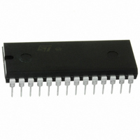
M48T35-70PC1 STMicroelectronics, M48T35-70PC1 Datasheet - Page 10

M48T35-70PC1
Manufacturer Part Number
M48T35-70PC1
Description
IC TIMEKPR NVRAM 256KBIT 5V 28DI
Manufacturer
STMicroelectronics
Series
Timekeeper®r
Type
Clock/Calendar/NVSRAMr
Datasheet
1.M48T35Y-70MH1E.pdf
(28 pages)
Specifications of M48T35-70PC1
Memory Size
256K (32K x 8)
Time Format
HH:MM:SS (24 hr)
Date Format
YY-MM-DD-dd
Interface
Parallel
Voltage - Supply
4.75 V ~ 5.5 V
Operating Temperature
0°C ~ 70°C
Mounting Type
Through Hole
Package / Case
28-DIP Module (600 mil), 28-EDIP
Function
Clock/Calendar/NV Timekeeping RAM/Watchdog Timer/Battery Backup
Rtc Memory Size
32768 Byte
Supply Voltage (max)
5.5 V
Supply Voltage (min)
4.75 V
Maximum Operating Temperature
+ 70 C
Minimum Operating Temperature
0 C
Mounting Style
Through Hole
Rtc Bus Interface
Parallel
Bus Type
Parallel
User Ram
32KB
Operating Supply Voltage (typ)
5V
Package Type
PCDIP
Operating Supply Voltage (max)
5.5V
Operating Supply Voltage (min)
4.75V
Operating Temperature Classification
Commercial
Operating Temperature (max)
70C
Operating Temperature (min)
0C
Pin Count
28
Mounting
Through Hole
Lead Free Status / RoHS Status
Lead free / RoHS Compliant
Other names
497-2845-5
Available stocks
Company
Part Number
Manufacturer
Quantity
Price
Company:
Part Number:
M48T35-70PC1
Manufacturer:
STMicroelectronics
Quantity:
135
Company:
Part Number:
M48T35-70PC1
Manufacturer:
STM
Quantity:
1 400
Part Number:
M48T35-70PC1
Manufacturer:
ST
Quantity:
20 000
Operation modes
2.2
Figure 6.
Figure 7.
10/28
A0-A14
E
W
DQ0-DQ7
A0-A14
E
W
DQ0-DQ7
WRITE mode
The M48T35/Y is in the WRITE mode whenever W and E are low. The start of a WRITE is
referenced from the latter occurring falling edge of W or E. A WRITE is terminated by the
earlier rising edge of W or E. The addresses must be held valid throughout the cycle. E or W
must return high for a minimum of t
to the initiation of another READ or WRITE cycle. Data-in must be valid t
end of WRITE and remain valid for t
cycles to avoid bus contention; although, if the output bus has been activated by a low on E
and G, a low on W will disable the outputs t
WRITE enable controlled, WRITE AC waveform
Chip enable controlled, WRITE AC waveforms
tAVEL
tAVEL
tAVWL
tAVWL
tWLQZ
Doc ID 2611 Rev 9
tAVWH
tAVEH
EHAX
tWLWH
VALID
tAVAV
VALID
tAVAV
WHDX
tELEH
from chip enable or t
afterward. G should be kept high during WRITE
WLQZ
tDVEH
tDVWH
DATA INPUT
after W falls.
DATA INPUT
tWHDX
WHAX
tEHDX
tWHQX
tEHAX
from WRITE enable prior
tWHAX
M48T35, M48T35Y
DVWH
prior to the
AI00926
AI00927


