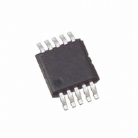
ISL1209IU10Z Intersil, ISL1209IU10Z Datasheet - Page 11

ISL1209IU10Z
Manufacturer Part Number
ISL1209IU10Z
Description
IC RTC LP BATT BACK SRAM 10MSOP
Manufacturer
Intersil
Type
Clock/Calendar/NVSRAMr
Datasheet
1.ISL1209IU10Z-TK.pdf
(24 pages)
Specifications of ISL1209IU10Z
Memory Size
2B
Time Format
HH:MM:SS (12/24 hr)
Date Format
YY-MM-DD-dd
Interface
I²C, 2-Wire Serial
Voltage - Supply
2.7 V ~ 5.5 V
Operating Temperature
-40°C ~ 85°C
Mounting Type
Surface Mount
Package / Case
10-MSOP, Micro10™, 10-uMAX, 10-uSOP
Lead Free Status / RoHS Status
Lead free / RoHS Compliant
Available stocks
Company
Part Number
Manufacturer
Quantity
Price
Company:
Part Number:
ISL1209IU10Z-TK
Manufacturer:
Intersil
Quantity:
47 631
Company:
Part Number:
ISL1209IU10Z-TK
Manufacturer:
Intersil
Quantity:
625
I
The ISL1209 has an I
access to the control and status registers and the user
SRAM. The I
industry I
signal (SDA) and a clock signal (SCL).
Oscillator Compensation
The ISL1209 provides the option of timing correction due to
temperature variation of the crystal oscillator for either
manufacturing calibration or active calibration. The total
possible compensation is typically -94ppm to +140ppm. Two
compensation mechanisms that are available are as follows:
Also provided is the ability to adjust the crystal capacitance
when the ISL1209 switches from V
mode. (See Battery Mode ATR Selection for more details.)
Register Descriptions
The battery-backed registers are accessible following a
slave byte of “1101111x” and reads or writes to addresses
[00h:13h]. The defined addresses and default values are
described in the Table 1. Address 09h is not used. Reads or
writes to 09h will not affect operation of the device but should
be avoided.
REGISTER ACCESS
The contents of the registers can be modified by performing
a byte or a page write operation directly to any register
address.
The registers are divided into 4 sections. These are:
There are no addresses above 13h.
Write capability is allowable into the RTC registers (00h to
06h) only when the WRTC bit (bit 4 of address 07h) is set to
“1”. A multi-byte read or write operation is limited to one
section per operation. Access to another section requires a
new operation. A read or write can begin at any address
within the section.
2
1. An analog trimming (ATR) register that can be used to
2. A digital trimming register (DTR) that can be used to
1. Real Time Clock (7 bytes): Address 00h to 06h.
2. Control and Status (5 bytes): Address 07h to 0Bh.
3. Alarm (6 bytes): Address 0Ch to 11h.
4. User SRAM (2 bytes): Address 12h to 13h.
C Serial Interface
adjust individual on-chip digital capacitors for oscillator
capacitance trimming. The individual digital capacitor is
selectable from a range of 9pF to 40.5pF (based upon
32.758kHz). This translates to a calculated
compensation of approximately -34ppm to +80ppm. (See
ATR description.)
adjust the timing counter by ±60ppm. (See DTR
description.)
2
C serial bus protocols using a bidirectional data
2
C serial interface is compatible with other
2
C serial bus interface that provides
11
DD
to battery backup
ISL1209
A register can be read by performing a random read at any
address at any time. This returns the contents of that register
location. Additional registers are read by performing a
sequential read. For the RTC and Alarm registers, the read
instruction latches all clock registers into a buffer, so an
update of the clock does not change the time being read. A
sequential read will not result in the output of data from the
memory array. At the end of a read, the master supplies a
stop condition to end the operation and free the bus. After a
read, the address remains at the previous address +1 so the
user can execute a current address read and continue
reading the next register.
It is not necessary to set the WRTC bit prior to writing into
the control and status, alarm, and user SRAM registers.
October 17, 2006
FN6109.4


