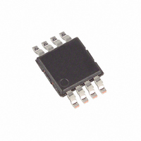
DS1371U+ Maxim Integrated Products, DS1371U+ Datasheet

DS1371U+
Specifications of DS1371U+
Related parts for DS1371U+
DS1371U+ Summary of contents
Page 1
... I C Serial Interface Low-Voltage Operation Operating Temperature Range: -40°C to +85°C Available in 8-Pin μSOP 2 C bidirectional Ordering Information PART DS1371U DS1371U+ + Denotes a lead-free/RoHS-compliant package appears on the top mark for lead-free packages. Pin Configuration TOP VIEW DS1371 Watchdog Clock PIN- TEMP RANGE PACKAGE -40° ...
Page 2
ABSOLUTE MAXIMUM RATINGS Voltage Range on V Pin Relative to Ground………………………………………………………..-0.3V to +6.0V CC Voltage Range on SDA, SCL, and WDS Relative to Ground…………………………………..-0. Operating Temperature Range (noncondensing)……………………………………………………...-40°C to +85°C Storage Temperature Range………………………………………………………………………….-55°C to +125°C Soldering Temperature…………………………………………………………………...See IPC/JEDEC ...
Page 3
AC ELECTRICAL CHARACTERISTICS (V = 1.7V to 5.5V -40°C to +85°C, unless otherwise noted.) (Note PARAMETER SCL Clock Frequency (Note 9) Bus Free Time Between STOP and START Conditions Hold Time (repeated) START Condition (Note ...
Page 4
Typical Operating Characteristics (V = 3.3V +25°C, unless otherwise noted 600 550 500 450 400 350 300 1.5 2.0 2.5 I OSC0 750 700 650 600 550 500 -40 -20 I OSC0 ...
Page 5
Figure 1. Timing Diagram X1 X2 Oscillator V CC Power GND WDS SDA Interface SCL Figure 2. Functional Diagram 32,768Hz 8192Hz 4096Hz 1Hz ÷4 ÷2 ÷4096 DS1371 1Hz WACE Alarm/ 4096Hz M Watchdog 1Hz U ÷4096 X ...
Page 6
PIN DESCRIPTION PIN NAME These signals are connections for a standard 32.768kHz quartz crystal. The internal oscillator circuitry is designed for operation with a crystal having a specified load capacitance ( X1, X2 information about crystal selection and ...
Page 7
Table 1. Crystal Specifications PARAMETER Nominal Frequency Series Resistance Load Capacitance *The crystal, traces, and crystal input pins should be isolated from RF generating signals. Refer to Application Note 58: Crystal Considerations for Dallas Real-Time Clocks for additional specifications. LOCAL ...
Page 8
Address Map Table 2 shows the address map for the registers of the DS1371. During a multibyte access, when the address pointer reaches the end of the register space (08h), it wraps around to location 00h START, ...
Page 9
Time-of-Day Counter The time-of-day counter is a 32-bit up counter. The contents can be read or written by accessing the address range 00h–03h. When the counter is read, the current time of day is latched into a register, which is ...
Page 10
Special Purpose Registers The DS1371 has two additional registers (07h–08h) that control the WD/ALM counter, square-wave output, and interrupts. Control Register (07h) Bit # 7 6 EOSC Name WACE Default 0 0 Bit 7: Enable Oscillator (EOSC). When set to ...
Page 11
Status Register (08h) Bit # 7 Name OSF Default 1 Bit 7: Oscillator Stop Flag (OSF). A logic 1 in this bit indicates that the oscillator either is stopped or was stopped for some period and can be used to ...
Page 12
Data valid: The state of the data line represents valid data when, after a START condition, the data line is stable for the duration of the high period of the clock signal. The data on the line must be changed ...
Page 13
Figures 5 and 6 detail how data transfer is accomplished on the I R/W bit, two types of data transfer are possible: Data transfer from a master transmitter to a slave receiver. The first byte transmitted by the master is ...
Page 14
Address> <Word Address (n)> XXXXXXXX A 1101000 B - Block Select Master to slave S - Start A - Acknowledge (ACK) Slave to master P - Stop 2 Figure Write Protocol <Slave Address> ...
Page 15
... Maxim/Dallas Semiconductor cannot assume responsibility for use of any circuitry other than circuitry entirely embodied in a Maxim/Dallas Semiconductor product. No circuit patent licenses are implied. Maxim/Dallas Semiconductor reserves the right to change the circuitry and specifications without notice at any time The Maxim logo is a registered trademark of Maxim Integrated Products, Inc. The Dallas logo is a registered trademark of Dallas Semiconductor Corporation. DESCRIPTION 2 C ...


