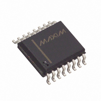
DS3231SN# Maxim Integrated Products, DS3231SN# Datasheet - Page 6

DS3231SN#
Manufacturer Part Number
DS3231SN#
Description
IC RTC W/TCXO 16-SOIC
Manufacturer
Maxim Integrated Products
Type
Clock/Calendar/TCXO/Crystalr
Datasheet
1.DS3231S.pdf
(20 pages)
Specifications of DS3231SN#
Time Format
HH:MM:SS (12/24 hr)
Date Format
YY-MM-DD-dd
Interface
I²C, 2-Wire Serial
Voltage - Supply
2.3 V ~ 5.5 V
Operating Temperature
-40°C ~ 85°C
Mounting Type
Surface Mount
Package / Case
16-SOIC (0.300", 7.5mm Width)
Function
Clock/Calendar/Battery Backup
Supply Voltage (max)
5.5 V
Supply Voltage (min)
2.3 V
Maximum Operating Temperature
+ 85 C
Minimum Operating Temperature
- 40 C
Mounting Style
SMD/SMT
Rtc Bus Interface
Serial (I2C)
Lead Free Status / RoHS Status
Lead free / RoHS Compliant
Memory Size
-
Lead Free Status / Rohs Status
Lead free / RoHS Compliant
Available stocks
Company
Part Number
Manufacturer
Quantity
Price
Extremely Accurate I
RTC/TCXO/Crystal
WARNING: Negative undershoots below -0.3V while the part is in battery-backed mode may cause loss of data.
Note 2: Limits at -40°C are guaranteed by design and not production tested.
Note 3: All voltages are referenced to ground.
Note 4: I
Note 5: Current is the averaged input current, which includes the temperature conversion current.
Note 6: The RST pin has an internal 50kΩ (nominal) pullup resistor to V
Note 7: After this period, the first clock pulse is generated.
Note 8: A device must internally provide a hold time of at least 300ns for the SDA signal (referred to the V
Note 9: The maximum t
Note 10: A fast-mode device can be used in a standard-mode system, but the requirement t
Note 11: C
Note 12: The parameter t
Note 13: This delay applies only if the oscillator is enabled and running. If the EOSC bit is a 1, t
6
SDA
SCL
NOTE: TIMING IS REFERENCED TO V
_____________________________________________________________________
STOP
to bridge the undefined region of the falling edge of SCL.
is automatically the case if the device does not stretch the low period of the SCL signal. If such a device does stretch the
low period of the SCL signal, it must output the next data bit to the SDA line t
before the SCL line is released.
0.0V ≤ V
ately goes high. The state of RST does not affect the I
CCA
B
t
BUF
—total capacitance of one bus line in pF.
—SCL clocking at max frequency = 400kHz.
START
CC
t
HD:STA
≤ V
IL(MAX)
CC(MAX)
HD:DAT
OSF
t
LOW
AND V
is the period of time the oscillator must be stopped for the OSF flag to be set over the voltage range of
IH(MIN)
needs only to be met if the device does not stretch the low period (t
and 2.3V ≤ V
t
R
.
t
HD:DAT
BAT
≤ 3.4V.
t
HIGH
t
F
2
t
SU:DAT
C-Integrated
2
C interface, RTC, or TCXO.
REPEATED
CC
START
Data Transfer on I
.
t
SU:STA
t
HD:STA
R(MAX)
SU:DAT
+ t
REC
SU:DAT
is bypassed and RST immedi-
≥ 250ns must then be met. This
LOW
= 1000 + 250 = 1250ns
) of the SCL signal.
t
SP
IH(MIN)
2
C Serial Bus
of the SCL signal)
t
SU:STO


