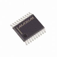
DS1315E-5+ Maxim Integrated Products, DS1315E-5+ Datasheet

DS1315E-5+
Specifications of DS1315E-5+
Related parts for DS1315E-5+
DS1315E-5+ Summary of contents
Page 1
DESCRIPTION The DS1315 Phantom Time combination of a CMOS timekeeper and a nonvolatile memory controller. In the absence of power, an external battery timekeeping operation and provides power for a CMOS static RAM. The watch keeps track of ...
Page 2
... DS1315EN-33 -40°C to +85°C DS1315EN-33+ -40°C to +85°C DS1315EN-33/T&R -40°C to +85°C DS1315EN-33+T&R -40°C to +85°C DS1315E-5 0°C to +70°C DS1315E-5+ 0°C to +70°C DS1315EN-5 -40°C to +85°C DS1315EN-5+ -40°C to +85°C DS1315EN-5/T&R -40°C to +85°C DS1315EN-5+T&R -40°C to +85°C DS1315S-33 0° ...
Page 3
Figure 1. Block Diagram DS1315 Phantom Time Chip ...
Page 4
Operation Communication with the Time Chip is established by pattern recognition of a serial bit stream of 64 bits which must be matched by executing 64 consecutive write cycles containing the proper data on data in (D). All accesses which ...
Page 5
Figure 2. Time Chip Comparison Register Definition Note: The pattern recognition in Hex is C5, 3A, A3, 5C, C5, 3A, A3, 5C. The odds of this pattern being accidentally duplicated and causing inadvertent entry to the Phantom Time Chip are ...
Page 6
Nonvolatile Controller Operation The operation of the nonvolatile controller circuits within the Time Chip is determined by the level of the ROM/ select pin. When ROM/ RAM and performs the circuit functions required to make CMOS RAM and the timekeeping ...
Page 7
Figure 4. ROM/Time Chip Interface Time Chip Register Information Time Chip information is contained in eight registers of 8 bits, each of which is sequentially accessed 1 bit at a time after the 64-bit pattern recognition sequence has been completed. ...
Page 8
Zero Bits Registers and 6 contain 1 or more bits that will always read logic 0. When writing these locations, either a logic acceptable. Figure 5. Time Chip Register Definition DS1315 ...
Page 9
ABSOLUTE MAXIMUM RATINGS Voltage Range on Any Pin Relative to Ground Operating Temperature Range, Commercial Operating Temperature Range, Industrial Storage Temperature Range Soldering Temperature This is a stress rating only and functional operation of the device at these or any ...
Page 10
DC POWER-DOWN ELECTRICAL CHARACTERISTICS (V < 4.5V Over the operating range PARAMETER Output Voltage CEO Battery BAT1 BAT2 Current Battery Backup Current @ -0.2V CCO BAT AC ELECTRICAL OPERATING CHARACTERISTICS—ROM/ ...
Page 11
AC ELECTRICAL OPERATING CHARACTERISTICS—ROM 5.0V ±10 Over the operating range PARAMETER Read Cycle Time Access Time CEI Access Time OE to Output Low Z CEI to Output Low Output High Z ...
Page 12
DC POWER-DOWN ELECTRICAL CHARACTERISTICS (V < 2.97V Over the operating range PARAMETER Output Voltage CEO Battery Current BAT1 BAT2 Battery Backup Current 0.2 CCO BAT AC ELECTRICAL OPERATING ...
Page 13
AC ELECTRICAL OPERATING CHARACTERISTICS—ROM 3.3V ±10 Over the operating range PARAMETER Read Cycle Time Access Time CEI Access Time OE to Output Low-Z CEI to Output Low Output High-Z CEI to Output ...
Page 14
Figure 6. Timing Diagram: Read Cycle to Time Chip ROM/ RAM = GND Figure 7. Timing Diagram: Write Cycle to Time Chip ROM/ RAM = GND DS1315 Phantom Time Chip ...
Page 15
Figure 8. Timing Diagram: Read Cycle to Time Chip ROM/ RAM = V Figure 9. Timing Diagram: Write Cycle to Time Chip ROM/RAM = V CCO CCO DS1315 Phantom Time Chip ...
Page 16
Figure 10. Timing Diagram: Reset Pulse RST 5V DEVICE POWER-UP/POWER-DOWN CHARACTERISTICS— ROM GND RAM CCO (T = 0°C to +70°C) A PARAMETER Recovery Time at Power-Up V Slew Rate CC Power-Down V (max (min) PF ...
Page 17
Figure 12. 5V Power-Down Condition 3.3V DEVICE POWER-UP POWER-DOWN CHARACTERISTICS— ROM GND RAM CCO (T = 0°C to +70°C) A PARAMETER Recovery Time at Power-Up V Slew Rate CC Power-Down V (max (min ...
Page 18
NOTES: 1) All voltages are referenced to ground. 2) Measured with load shown in Figure 15. 3) Input pulse rise and fall times equal 10ns function of the latter occurring edge of WR mode ...
Page 19
Figure 14. 3.3V Power-Down Condition Figure 15. Output Load DS1315 Phantom Time Chip ...
Page 20
PIN CONFIGURATIONS (continued BAT1 4 GND GND 16-Pin SO (300 mil) PACKAGE INFORMATION For the latest package outline information and land patterns www.maxim-ic.com/packages. PACKAGE TYPE PACKAGE ...
Page 21
DIP PKG 16-PIN DIM. MIN A IN. 0.740 MM B IN. 0.240 MM C IN. 0.120 MM D IN. 0.300 MM E IN. 0.015 MM F IN. 0.110 MM G IN. 0.090 MM H IN. 0.300 MM J IN. ...
Page 22
SO PKG 16-PIN DIM MIN A IN. 0.402 MM 10.21 B IN. 0.290 MM 7.37 C IN. 0.089 MM 2.26 E IN. 0.004 MM 0.102 F IN. 0.094 MM 2.38 G IN. 0.050 BSC MM 1.27 BSC H IN. ...
Page 23
... Maxim/Dallas Semiconductor cannot assume responsibility for use of any circuitry other than circuitry entirely embodied in a Maxim/Dallas Semiconductor product. No circuit patent licenses are implied. Maxim/Dallas Semiconductor reserves the right to change the circuitry and specifications without notice at any time The Maxim logo is a registered trademark of Maxim Integrated Products, Inc. The Dallas logo is a registered trademark of Dallas Semiconductor Corporation. DIM A MM ...


