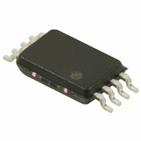
S-35190A-T8T1G Seiko Instruments, S-35190A-T8T1G Datasheet - Page 36

S-35190A-T8T1G
Manufacturer Part Number
S-35190A-T8T1G
Description
IC REAL TIME CLOCK 3WIRE 8-TSSOP
Manufacturer
Seiko Instruments
Type
Clock/Calendarr
Datasheet
1.S-35190A-J8T1G.pdf
(55 pages)
Specifications of S-35190A-T8T1G
Time Format
HH:MM:SS (12/24 hr)
Date Format
YY-MM-DD-dd
Interface
3-Wire Serial
Voltage - Supply
1.3 V ~ 5.5 V
Operating Temperature
-40°C ~ 85°C
Mounting Type
Surface Mount
Package / Case
8-TSSOP
Function
Clock/Calendar/Alarm/Battery Backup/Interrupt
Supply Voltage (max)
5.5 V
Supply Voltage (min)
1.3 V
Maximum Operating Temperature
+ 85 C
Minimum Operating Temperature
- 40 C
Mounting Style
SMD/SMT
Rtc Bus Interface
Serial (3-Wire)
Lead Free Status / RoHS Status
Lead free / RoHS Compliant
Memory Size
-
Lead Free Status / Rohs Status
Lead free / RoHS Compliant
Available stocks
Company
Part Number
Manufacturer
Quantity
Price
Part Number:
S-35190A-T8T1G
Manufacturer:
SEIKO
Quantity:
20 000
36
3-WIRE REAL-TIME CLOCK
S-35190A
Crystal oscillator: 32.768 kHz
Caution
Adjustment of Oscillation Frequency
1. Configuration of oscillation
Since crystal oscillation is sensitive to external noise (the clock accuracy is affected), the following measures are
essential for optimizing the oscillation configuration.
(1)
(2)
(3)
(4)
(5)
*1. When setting the value for the crystal oscillator’s C
*2. Design the board so that the parasitic capacitance is 5 pF.
*3. The oscillator operates unless C
advances.
C
C
Place the S-35190A, crystal oscillator, and external capacitor (C
Increase the insulation resistance between pins and the substrate wiring patterns of XIN and XOUT.
Do not place any signal or power lines close to the oscillator.
Locating the GND layer immediately below the oscillator is recommended.
Locate the bypass capacitor adjacent to the power supply pin of the S-35190A.
L
g
= 6 pF
= None
1. When using the crystal oscillator with a C
2. Oscillation characteristics are subject to the variation of each component such as substrate parasitic
oscillation operation may become unstable. Use a crystal oscillator with a C
capacitance, parasitic resistance, crystal oscillator, and C
sufficient attention for them.
*1
*2
Parasitic capacitance
to 9.1 pF
Parasitic capacitance
C
g
oscillator
Crystal
g
*3
is not connected. Note that the oscillation frequency is in the direction that it
Figure 44 Connection Diagram 1
Figure 45 Connection Diagram 2
*3
Seiko Instruments Inc.
C
g
XIN
XOUT
L
as 7 pF, connect C
C
d
1
2
3
4
L
Locate the GND layer in the
layer immediately below
exceeding the rated value (7 pF) (e.g : C
XIN
VSS
XOUT
S-35190A
g
) as close to each other as possible.
R
R
f
d
d
externally if necessary.
g
. When configuring oscillator, pay
8
7
6
5
S-35190A
Oscillation internal constant
standard values:
L
value of 6 pF or 7 pF.
R
R
C
f
d
d
= 100 MΩ
= 100 kΩ
= 8 pF
Rev.3.0
L
= 12.5 pF),
_00


