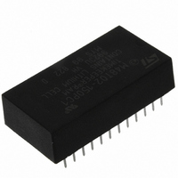
M48T02-150PC1 STMicroelectronics, M48T02-150PC1 Datasheet - Page 7

M48T02-150PC1
Manufacturer Part Number
M48T02-150PC1
Description
IC TIMEKPR NVRAM 16KBIT 5V 24-DI
Manufacturer
STMicroelectronics
Series
Timekeeper®r
Type
Clock/Calendar/NVSRAMr
Specifications of M48T02-150PC1
Memory Size
16K (2K x 8)
Time Format
HH:MM:SS (24 hr)
Date Format
YY-MM-DD-dd
Interface
Parallel
Voltage - Supply
4.75 V ~ 5.5 V
Operating Temperature
0°C ~ 70°C
Mounting Type
Through Hole
Package / Case
24-DIP (600 mil) Module
Function
Clock/Calendar/NV Timekeeping RAM/Battery Backup
Rtc Memory Size
2048 Byte
Supply Voltage (max)
5.5 V
Supply Voltage (min)
4.75 V
Maximum Operating Temperature
+ 70 C
Minimum Operating Temperature
0 C
Mounting Style
Through Hole
Rtc Bus Interface
Parallel
Capacitance, Input
10 pF
Capacitance, Output
10 pF
Current, Input, Leakage
±1 μA
Current, Operating
80 mA
Current, Output, Leakage
±1
Data Retention
10 yrs.
Density
16K
Memory Type
Non-Volatile SRAM
Organization
2K×8
Package Type
PCDIP24
Power Dissipation
1 W
Temperature, Operating
0 to +70 °C
Time, Access
150 ns
Time, Fall
≤5 ns
Time, Rise
≤5 ns
Voltage, Input, High
5.05 to 5.8 V
Voltage, Input, Low
0.8 V
Voltage, Output, High
2.4 V
Voltage, Output, Low
0.4 V
Voltage, Supply
4.75 to 5.5 V
Lead Free Status / RoHS Status
Lead free / RoHS Compliant
Other names
497-2825-5
Available stocks
Company
Part Number
Manufacturer
Quantity
Price
Company:
Part Number:
M48T02-150PC1
Manufacturer:
Maxim
Quantity:
58
Part Number:
M48T02-150PC1
Manufacturer:
ST
Quantity:
20 000
M48T02, M48T12
2
Note:
2.1
Operation modes
As
oscillator of the M48T02/12 are integrated on one silicon chip. The two circuits are
interconnected at the upper eight memory locations to provide user accessible
BYTEWIDE™ clock information in the bytes with addresses 7F8h-7FFh. The clock locations
contain the year, month, date, day, hour, minute, and second in 24-hour BCD format.
Corrections for 28, 29 (leap year - valid until 2100), 30, and 31 day months are made
automatically.
Byte 7F8h is the clock control register. This byte controls user access to the clock
information and also stores the clock calibration setting.
The eight clock bytes are not the actual clock counters themselves; they are memory
locations consisting of BiPORT™ READ/WRITE memory cells. The M48T02/12 includes a
clock control circuit which updates the clock bytes with current information once per second.
The information can be accessed by the user in the same manner as any other location in
the static memory array.
The M48T02/12 also has its own power-fail detect circuit. The control circuitry constantly
monitors the single 5 V supply for an out of tolerance condition. When V
tolerance, the circuit write protects the SRAM, providing a high degree of data security in the
midst of unpredictable system operation brought on by low V
approximately 3 V, the control circuitry connects the battery which maintains data and clock
operation until valid power returns.
Table 2.
1. See
X = V
READ mode
The M48T02/12 is in the READ mode whenever W (WRITE enable) is high and E (chip
enable) is low. The device architecture allows ripple-through access of data from eight of
16,384 locations in the static storage array. Thus, the unique address specified by the 11
Address Inputs defines which one of the 2,048 bytes of data is to be accessed. Valid data
will be available at the data I/O pins within address access time (t
address input signal is stable, providing that the E and G access times are also satisfied. If
the E and G access times are not met, valid data will be available after the latter of the chip
enable access time (t
Deselect
Deselect
Deselect
WRITE
READ
READ
Mode
Figure 3 on page 6
IH
Table 11 on page 20
or V
IL
Operating modes
; V
4.75 to 5.5 V
V
4.5 to 5.5 V
PFD
≤ V
SO
V
V
SO
or
(min)
SO
CC
= Battery backup switchover voltage.
to
ELQV
(1)
shows, the static memory array and the quartz controlled clock
(1)
for details.
) or output enable access time (t
Doc ID 2410 Rev 8
V
V
V
V
E
X
X
IH
IL
IL
IL
V
V
G
X
X
X
X
IH
IL
V
V
V
W
X
X
X
IH
IH
IL
DQ0-DQ7
GLQV
High Z
High Z
High Z
High Z
D
CC
D
OUT
IN
. As V
).
AVQV
CC
) after the last
Battery backup mode
CC
falls below
Operation modes
CMOS standby
is out of
Standby
Power
Active
Active
Active
7/25


