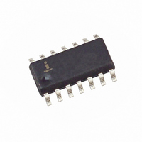
X1228S14 Intersil, X1228S14 Datasheet - Page 20

X1228S14
Manufacturer Part Number
X1228S14
Description
IC RTC CPU SUP WDT 4K EE 14-SOIC
Manufacturer
Intersil
Type
Clock/Calendar/EEPROMr
Datasheet
1.X1228S14-2.7A.pdf
(29 pages)
Specifications of X1228S14
Memory Size
4K (512 x 8)
Time Format
HH:MM:SS (12/24 hr)
Date Format
YY-MM-DD-dd
Interface
I²C, 2-Wire Serial
Voltage - Supply
2.7 V ~ 5.5 V
Operating Temperature
0°C ~ 70°C
Mounting Type
Surface Mount
Package / Case
14-SOIC (3.9mm Width), 14-SOL
Lead Free Status / RoHS Status
Contains lead / RoHS non-compliant
Available stocks
Company
Part Number
Manufacturer
Quantity
Price
Company:
Part Number:
X1228S14
Manufacturer:
Intersil
Quantity:
1
Part Number:
X1228S14I-2.7
Manufacturer:
INTERSIL
Quantity:
20 000
Part Number:
X1228S14I-4.5AT1
Manufacturer:
INTERSIL
Quantity:
20 000
Company:
Part Number:
X1228S14IZ
Manufacturer:
NXP
Quantity:
906
Part Number:
X1228S14IZ-2.7A
Manufacturer:
INTERSIL
Quantity:
20 000
Figure 10. Slave Address, Word Address, and Data Bytes (64 Byte pages)
Write Operations
Byte Write
For a write operation, the device requires the Slave
Address Byte and the Word Address Bytes. This gives
the master access to any one of the words in the array
or CCR. (Note: Prior to writing to the CCR, the master
must write a 02h, then 06h to the status register in two
preceding operations to enable the write operation.
See “Writing to the Clock/Control Registers.” Upon
receipt of each address byte, the X1228 responds with
an acknowledge. After receiving both address bytes
Figure 11. Byte Write Sequence
Figure 12. Writing 30 bytes to a 64-byte memory page starting at address 40.
Array
CCR
7 Bytes
Signals from
the Master
SDA Bus
Signals From
The Slave
Address
1
1
A7
D7
0
= 6
20
Device Identifier
0
1
A6
D6
0
D5
A5
1
0
0
Address Pointer
Ends Here
Addr = 7
S
a
t
r
t
1
Address
Slave
D4
A4
0
1
0
1
1
1
0
A3
D3
1
0
A
C
K
0 0 0 0 0 0 0
Address 1
X1228
Word
A2
D2
1
0
the X1228 awaits the eight bits of data. After receiving
the 8 data bits, the X1228 again responds with an
acknowledge. The master then terminates the transfer
by generating a stop condition. The X1228 then
begins an internal write cycle of the data to the nonvol-
atile memory. During the internal write cycle, the
device inputs are disabled, so the device will not
respond to any requests from the master. The SDA out-
put is at high impedance. See Figure 11.
Address
D1
A1
A
C
K
1
0
40
Address 0
Word
R/W
A8
A0
D0
Slave Address Byte
Byte 0
Word Address 1
Byte 1
Word Address 0
Byte 2
Data Byte
Byte 3
A
C
K
23 Bytes
Data
Address
A
C
K
63
S
o
p
t
May 18, 2006
FN8100.4


