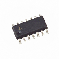
X1228S14 Intersil, X1228S14 Datasheet - Page 9

X1228S14
Manufacturer Part Number
X1228S14
Description
IC RTC CPU SUP WDT 4K EE 14-SOIC
Manufacturer
Intersil
Type
Clock/Calendar/EEPROMr
Datasheet
1.X1228S14-2.7A.pdf
(29 pages)
Specifications of X1228S14
Memory Size
4K (512 x 8)
Time Format
HH:MM:SS (12/24 hr)
Date Format
YY-MM-DD-dd
Interface
I²C, 2-Wire Serial
Voltage - Supply
2.7 V ~ 5.5 V
Operating Temperature
0°C ~ 70°C
Mounting Type
Surface Mount
Package / Case
14-SOIC (3.9mm Width), 14-SOL
Lead Free Status / RoHS Status
Contains lead / RoHS non-compliant
Available stocks
Company
Part Number
Manufacturer
Quantity
Price
Company:
Part Number:
X1228S14
Manufacturer:
Intersil
Quantity:
1
Part Number:
X1228S14I-2.7
Manufacturer:
INTERSIL
Quantity:
20 000
Part Number:
X1228S14I-4.5AT1
Manufacturer:
INTERSIL
Quantity:
20 000
Company:
Part Number:
X1228S14IZ
Manufacturer:
NXP
Quantity:
906
Part Number:
X1228S14IZ-2.7A
Manufacturer:
INTERSIL
Quantity:
20 000
DESCRIPTION
The X1228 device is a Real Time Clock with
clock/calendar, two polled alarms with integrated 512x8
EEPROM, oscillator compensation, CPU Supervisor
(POR/LVS and WDT) and battery backup switch.
The oscillator uses an external, low-cost 32.768kHz
crystal. All compensation and trim components are
integrated on the chip. This eliminates several external
discrete components and a trim capacitor, saving
board area and component cost.
The Real-Time Clock keeps track of time with
separate registers for Hours, Minutes, Seconds. The
Calendar has separate registers for Date, Month, Year
and Day-of-week.
2099, with automatic leap year correction.
The powerful Dual Alarms can be set to any
Clock/Calendar value for a match. For instance, every
minute, every Tuesday, or 5:23 AM on March 21. The
alarms can be polled in the Status Register or provide
a hardware interrupt (IRQ Pin).
mode for the alarms allowing a periodic interrupt.
The PHZ/IRQ pin may be software selected to provide
a frequency output of 1 Hz, 4096 Hz, or 32,768 Hz.
The X1228 device integrates CPU Supervisor func-
tions and a Battery Switch. There is a Power-On Reset
(RESET output) with typically 250 ms delay from
power-on. It will also assert RESET when Vcc goes
below the specified threshold. The V
user repro-grammable. There is a WatchDog Timer
(WDT) with 3 selectable time-out periods (0.25s,
0.75s, 1.75s) and a disabled setting. The watchdog
activates the RESET pin when it expires.
The device offers a backup power input pin. This
V
battery or SuperCap. The entire X1228 device is fully
operational
clock/calendar portion of the X1228 device remains
fully operational down to 1.8 volts (Standby Mode).
The X1228 device provides 4K bits of EEPROM with 8
modes of BlockLock™ control. The BlockLock allows a
safe, secure memory for critical user and configuration
data, while allowing a large user storage area.
BACK
pin allows the device to be backed up by
from
The calendar is correct through
2.7
to
9
5.5
There is a repeat
volts
trip
threshold is
and
the
X1228
PIN DESCRIPTIONS
Serial Clock (SCL)
The SCL input is used to clock all data into and out of
the device. The input buffer on this pin is always active
(not gated).
Serial Data (SDA)
SDA is a bidirectional pin used to transfer data into
and out of the device. It has an open drain output and
may be wire ORed with other open drain or open col-
lector outputs. The input buffer is always active (not
gated).
An open drain output requires the use of a pull-up
resistor. The output circuitry controls the fall time of
the output signal with the use of a slope controlled
pull-down. The circuit is designed for 400kHz 2-wire
interface speeds.
V
This input provides a backup supply voltage to the
device. V
event the V
to a battery, a Supercap or tied to ground if not used.
RESET Output – RESET
This is a reset signal output. This signal notifies a host
processor that the watchdog time period has expired or
that the voltage has dropped below a fixed V
old. It is an open drain active LOW output. Recom-
mended value for the pullup resistor is 5kΩ. If unused, tie
to ground.
Programmable Frequency/Interrupt Output – PHZ/IRQ
This is either an output from the internal oscillator or an
interrupt signal output. It is a CMOS output.
When used as frequency output, this signal has a fre-
quency of 32.768kHz, 4096Hz, 1Hz or inactive.
When used as interrupt output, this signal notifies a
host processor that an alarm has occurred and an
action is required. It is an active LOW output.
The control bits for this function are FO1 and FO0 and
are found in address 0011h of the Clock Control Mem-
ory map. See “Programmable Frequency Output
Bits—FO1, FO0” on page 14.
NC = No internal connection
BACK
BACK
CC
RESET
supply fails. This pin can be connected
V
NC
NC
NC
supplies power to the device in the
X1
X2
SS
14 LD TSSOP/SOIC
1
2
3
4
5
6
7
X1228
14
13
12
11
10
9
8
V
V
PHZ/IRQ
NC
NC
SCL
SDA
CC
BACK
TRIP
May 18, 2006
thresh-
FN8100.4


