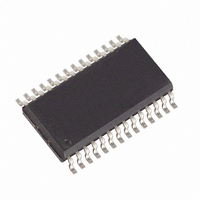
DS1689S-TRL Maxim Integrated Products, DS1689S-TRL Datasheet - Page 3

DS1689S-TRL
Manufacturer Part Number
DS1689S-TRL
Description
IC RTC SER W/NV RAM CTRL 28-SOIC
Manufacturer
Maxim Integrated Products
Type
Clock/Calendar/Serializedr
Datasheet
1.DS1689S.pdf
(36 pages)
Specifications of DS1689S-TRL
Memory Size
114B
Time Format
HH:MM:SS (12/24 hr)
Date Format
YY-MM-DD-dd
Interface
Parallel
Voltage - Supply
2.7 V ~ 3.3 V, 4.5 V ~ 5.5 V
Operating Temperature
0°C ~ 70°C
Mounting Type
Surface Mount
Package / Case
28-SOIC (7.5mm Width)
Lead Free Status / RoHS Status
Contains lead / RoHS non-compliant
14, 19
SO
13
15
16
17
18
20
21
22
23
PIN
EDIP
13
14
15
16
17
18
20
21
22
—
NAME
PSEL
PWR
GND
V
ALE
IRQ
WR
RD
KS
CS
BAT
Active-Low Power-On Interrupt Output. The PWR pin is intended
for use as an on/off control for the system power. With V
removed from the DS1689/DS1693, PWR may be automatically
activated from a kickstart input via the KS pin or from a wake-up
interrupt. Once the system is powered on, the state of PWR can be
controlled via bits in the Dallas registers.
Ground. DC power is provided to the device on this pin.
Active-Low Kickstart Input. When V
DS1689/DS1693, the system can be powered on in response to an
active low transition on the KS pin, as might be generated from a
key closure. V
(ABE) must be set to 1 if the kickstart function is used, and the KS
pin must be pulled up to the V
KS pin can be used as an interrupt input.
Active-Low Chip Select Input. This signal must be asserted low
during a bus cycle for the RTC portion of the DS1689/DS1693 to be
accessed. CS must be kept in the active state during RD and WR
timing. Bus cycles, which take place with ALE asserted but without
asserting, CS will latch addresses. However, no data transfer will
occur.
Address Strobe Input (Active High). A pulse on the address strobe
pin serves to demultiplex the bus. The falling edge of ALE causes
the RTC address to be latched within the DS1689/DS1693.
Active-Low Write Data Strobe. The WR signal is an active low
signal. The WR signal defines the time period during which data is
written to the addressed register.
Active-Low Read Data Strobe. RD identifies the time period when
the DS1689/DS1693 drives the bus with RTC read data. The RD
signal is an enable signal for the output buffers of the clock.
+3V or +5V Power Select. When PSEL is logic 1, 5V operation is
selected. When PSEL is logic 0 or is floated, the device is in
autosense mode and determines the correct mode of operation based
on the voltage on V
Active-Low Interrupt Request Output (Open Drain). The IRQ pin is
an active-low output of the DS1689/DS1693 that can be tied to the
interrupt input of a processor. The IRQ output remains low as long
as the status bit causing the interrupt is present and the
corresponding interrupt-enable bit is set. To clear the IRQ pin, the
application software must clear all enabled flag bits contributing to
IRQ’s active state. When no interrupt conditions are present, the IRQ
level is in the high impedance state. Multiple interrupting devices
can be connected to an IRQ bus. The IRQ pin is an open-drain
output and requires an external pullup resistor.
Battery Input for Any Standard 3V Lithium Cell or Other Energy
Source. Battery voltage must be held between 2.5V and 3.7V for
proper operation.
BAUX
3 of 36
CCI
must be present and auxiliary battery enable bit
.
FUNCTION
BAUX
supply. While V
CC
is removed from the
CC
is applied, the
CC
voltage


