DS1689S-TRL Maxim Integrated Products, DS1689S-TRL Datasheet - Page 33

DS1689S-TRL
Manufacturer Part Number
DS1689S-TRL
Description
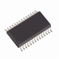
IC RTC SER W/NV RAM CTRL 28-SOIC
Manufacturer
Maxim Integrated Products
Type
Clock/Calendar/Serializedr
Datasheet
1.DS1689S.pdf
(36 pages)
Specifications of DS1689S-TRL
Memory Size
114B
Time Format
HH:MM:SS (12/24 hr)
Date Format
YY-MM-DD-dd
Interface
Parallel
Voltage - Supply
2.7 V ~ 3.3 V, 4.5 V ~ 5.5 V
Operating Temperature
0°C ~ 70°C
Mounting Type
Surface Mount
Package / Case
28-SOIC (7.5mm Width)
Lead Free Status / RoHS Status
Contains lead / RoHS non-compliant
NOTES:
1) All voltages are referenced to ground.
2) Typical values are at +25°C and nominal supplies.
3) Outputs are open.
4) Value for voltage and currents is from the V
5) Write protection trip point occurs during power fail prior to switchover from V
6) Value for voltage and currents is from the V
7) Applies to the AD0–AD7 pins, and the SQW pin when each is in a high impedance state.
8) The IRQ pin is open drain.
9) Measured with a load of 50pF + 1 TTL gate.
10) Wake-up/kickstart timeout generated only when the oscillator is enabled and the countdown chain is
11) V
12) Z
13) The DS1693 keeps time to an accuracy of ±1 minute per month during data retention time for the
14) t
15) The CEI pin has an internal pullup of 60kΩ.
16) The PSEL pin has an internal pulldown of 60kΩ.
17) For industrial grade parts, I
18) Real-time clock modules can be successfully processed through conventional wave-soldering
not reset.
4mA is forced through Z
period of t
registers of the DS1693. As such, t
SRAM, an auxiliary battery must be connected to the V
such that it can power the external SRAM for the t
techniques as long as temperature exposure to the lithium energy source contained within does not
exceed +85°C. Post solder cleaning with water washing techniques is acceptable, provided that
ultrasonic vibration is not used.
DR
CE
SW
is the amount of time that the internal battery can power the internal oscillator and internal
is an average input to output impedance as the input is swept from GND to V
is determined by the larger of V
DR
.
CE
.
BAT
(with OSC off) limit increases to 250nA.
DR
BAT
is specified with V
and V
CCI
BAT
BAUX
input pin to the V
input pin to the V
33 of 36
DR
.
period.
BAUX
CCO
floating. If V
pin. The auxiliary battery should be sized
CCO
CCO
pin.
pin.
CCO
is powering an external
CC
CCI
to V
and less than
BAT
.


