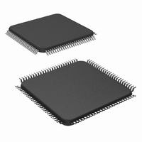
LM9833CCVJD/NOPB National Semiconductor, LM9833CCVJD/NOPB Datasheet - Page 3

LM9833CCVJD/NOPB
Manufacturer Part Number
LM9833CCVJD/NOPB
Description
IC USB IMAGE SCAN 48BIT 100-TOFP
Manufacturer
National Semiconductor
Datasheet
1.LM9833CCVJDNOPB.pdf
(42 pages)
Specifications of LM9833CCVJD/NOPB
Number Of Bits
16
Number Of Channels
3
Voltage - Supply, Analog
5V
Voltage - Supply, Digital
4.5 V ~ 5.5 V
Package / Case
100-TQFP, 100-VQFP
Lead Free Status / RoHS Status
Lead free / RoHS Compliant
Power (watts)
-
Other names
*LM9833CCVJD
*LM9833CCVJD/NOPB
LM9833CCVJD
*LM9833CCVJD/NOPB
LM9833CCVJD
Pin Descriptions
D+, D-
BUS POWER
ACTIVE/
SUSPENDED
SDA
SCL
OS
OS
OS
V
V
V
V
D0 (LSB) -D15
(MSB)
RD
WR
A0-A9
RAS
CAS
PAPER
SENSE 1-2
MISC I/O 1-6
REF LO
REF MID
REF HI
BANDGAP
R
G
B
,
,
Scanner Support I/O
Digital I/O. USB Interface signals
Digital Input. Tie low for bus powered sys-
tems, tie high for external power.
Digital Output. Low in Suspend mode. High in
operational mode. Used to control external
regulators, other components.
Digital I/O. Serial Data to/from external
EEPROM.
Digital Output. Serial Clock Output to external
EEPROM.
Analog Inputs. These inputs (for Red, Green,
and Blue) should be tied to the sensor’s out-
put signal through DC blocking capacitors. If
unused, tie to ground through DC blocking
capacitors.
Analog Output/Input. Bypass to AGND with a
0.047µF monolithic capacitor. Do not put a
DC load on this pin.
Analog Output/Input. Bypass to AGND with a
0.047µF monolithic capacitor. Do not put a
DC load on this pin.
Analog Output/Input. Bypass to AGND with a
0.047µF monolithic capacitor. Do not put a
DC load on this pin.
Analog Output. Bypass to AGND with a
0.047µF monolithic capacitor. Do not put a
DC load on this pin.
Digital Inputs/Outputs. This is the 16 bit data
path between the external DRAM and the
LM9833.
Digital Output. Read signal to external DRAM.
Digital Output. Write signal to external DRAM.
Digital Outputs. Address pins for up to 1M x
16 external DRAM.
Digital Output. Row Address Strobe signal.
Digital Output. Column Address Strobe sig-
nal.
Digital Inputs. Programmable, used for sens-
ing
switches, etc.
Digital Inputs/Outputs. Programmable, used
for front panel switches, status LEDs, etc. At
power-on and in Suspend Mode, MISC I/Os
1-3 are inputs and MISC I/Os 4-6 are outputs.
USB Interface
home
Analog
DRAM
position,
paper,
front
panel
3
A, B, A, B
SENSE
SENSE
SENSE
ø1
ø2
RS
CP1
CP2
TR1, TR2
LAMP
LAMP
LAMP
CRYSTAL IN
CRYSTAL
OUT
CRYSTAL/
EXT CLOCK
24/48
V
RESET
TEST
CMODE
REGULATOR
R
G
B
,
,
A
B
GND
,
Master Clock Generation
Digital Outputs. Pulses to stepper motor drive
circuitry.
Analog Inputs. Current sensing for stepper
motor’s PWM current control.
Analog Input. Ground sense input for stepper
motor’s PWM current control.
Digital Output. CCD/CIS clock signal phase 1.
Digital Output. CCD/CIS clock signal phase 2.
Digital Output. Reset pulse for the CCD/CIS.
Digital Output. Clamp pulse for the CCD/CIS.
Digital Output. Clamp pulse for the CCD/CIS.
Digital Outputs. Transfer pulses for the
CCD/CIS.
Digital Outputs. Used to control R, G, and B
LEDs of single output CIS, as well as bright-
ness of CCFL. The CDS signal can be seen
on LAMP
7).
Digital Input. Used with CRYSTAL OUT and
an external 48MHz crystal to form a crystal
oscillator.
Digital Output. Used with CRYSTAL IN and an
external 48MHz crystal to form a crystal oscil-
lator.
Digital Input. Tie to DGND for operation with
an external crystal. Pull up to V
CRYSTAL OUT with an external TTL or
CMOS clock source.
Digital Input. Tie to DGND for operation with a
48MHz crystal or external clock. Pull up to V
for operation with a 24MHz crystal or external
clock. NOTE: Operation at 24MHz is not guar-
anteed - always use a 48MHz crystal.
Digital Output. This is the regulated 3.3V sup-
ply (generated from V
transceiver. It should be used as the terminal
voltage for the 1.5k D+ pullup resistor, and
bypassed to DGND with a 0.047µF monolithic
capacitor.
Digital input. Take high to force device into
Power On Reset state, low to exit reset state.
Analog Output.
Digital Input. Test mode, always tie high.
Sensor Control
Stepper Motor
Miscellaneous
B
in a test mode (see register 5E, bit
D
) that powers the USB
www.national.com
D
to drive
D


