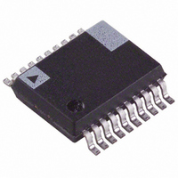
AD73311LARS Analog Devices Inc, AD73311LARS Datasheet - Page 30

AD73311LARS
Manufacturer Part Number
AD73311LARS
Description
IC ANALOG FRONT END 20-SSOP
Manufacturer
Analog Devices Inc
Datasheet
1.AD73311LAR.pdf
(36 pages)
Specifications of AD73311LARS
Rohs Status
RoHS non-compliant
Number Of Bits
16
Number Of Channels
2
Power (watts)
50mW
Voltage - Supply, Analog
3V
Voltage - Supply, Digital
3V
Package / Case
20-SSOP
Available stocks
Company
Part Number
Manufacturer
Quantity
Price
Company:
Part Number:
AD73311LARS
Manufacturer:
AD
Quantity:
12
Part Number:
AD73311LARS
Manufacturer:
ADI/亚德诺
Quantity:
20 000
Company:
Part Number:
AD73311LARS/AD73311
Manufacturer:
LITEON
Quantity:
10 000
Company:
Part Number:
AD73311LARSREEL
Manufacturer:
STM
Quantity:
6 706
Company:
Part Number:
AD73311LARSZ
Manufacturer:
MIC
Quantity:
6 222
Part Number:
AD73311LARSZ
Manufacturer:
ADI/亚德诺
Quantity:
20 000
Part Number:
AD73311LARSZ-REEL
Manufacturer:
ADI/亚德诺
Quantity:
20 000
AD73311L
Configuring an AD73311L to Operate in Mixed Mode
This section describes a typical sequence of control words that
would be sent to an AD73311L to configure it for operation in
mixed mode. It is not intended to be a definitive initialization
sequence, but will show users the typical input/output events
that occur in the programming and Operation Phases
description panel refers to Table XX.
Steps 1–3 detail the transfer of the control words to Control
Register A, which programs the device for Mixed-Mode opera-
tion. In Step 1, we have the first output sample event following
device reset. The SDOFS signal is raised which prepares the
DSP Rx register to accept the ADC word from the AD73311L.
The device is configured as nonFSLB, which means that the
DSP has control over what is transmitted to the device and in
this case we will not transmit to the device until the output word
has been received from the AD73311L.
In Step 2 the DSP has now received the ADC word. Typically,
an interrupt will be generated following reception of the output
words by the DSP. The transmit register of the DSP is loaded
with the control word destined for the AD73311L. This gener-
ates a transmit frame-sync (TFS) that is input to the SDIFS
input of the AD73311L to indicate the start of transmission.
In Step 3 the device has received a control word that addresses
Control Register A and programs the channels into Mixed
Mode-MM and PGM/DATA set to one. Following Step 3, the
device has been programmed into mixed-mode although none of
the analog sections have been powered up (controlled by Con-
trol Register C). Steps 4–6 detail update of Control Register B
in mixed-mode. In Steps 4, 5 the ADC sample, which is invalid
as the ADC section is not yet powered up, is transferred to the
DSP’s Rx section. In the subsequent interrupt service routine
1
. This
APPENDIX B
the Tx register is loaded with the control word setting for Con-
trol Register B which programs DMCLK = MCLK, the sam-
pling rate to DMCLK/256, SCLK = DMCLK/2.
Steps 7–10 are similar to Steps 4–6 except that Control Register
C is programmed to power up all analog sections (ADC, DAC,
Reference = 1.2 V, REFOUT). In Step 10, a DAC word is sent
to the device. As the channels are in mixed mode, the serial port
interrogates the MSB of the 16-bit word sent to determine whether
it contains DAC data or control information.
Steps 7–10 illustrate the implementation of Control Register
update and DAC update in a single sample period. Note that
this combination is not possible in the FSLB configuration
Steps 11–15 illustrate a Control Register readback cycle. In Step
13, the device has received a Control Word that addresses Con-
trol Register C for readback (Bit 14 of the Control Word = 1).
When the device receives the readback request, the register
contents are loaded to the serial register as shown in Step 14.
SDOFS is raised in the device, which causes the readback word
to be shifted out toward the DSP. In Step 15, the DSP has
received the readback word (note that the address field in the
readback word has been decremented to 111b). Steps 16–18
detail an ADC and DAC update cycle using the nonFSLB con-
figuration. In this case no Control Register update is required.
NOTES
1
2
This sequence assumes that the DSP SPORT's Rx and Tx interrupts are enabled.
Mixed mode operation with the FSLB configuration is more restricted in that
It is important to ensure there is no latency (separation) between control words
in a cascade configuration. This is especially the case when programming
Control Registers A and B.
only a single word can be sent per sample period.
2
.


