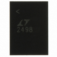
LTC2498IUHF#PBF Linear Technology, LTC2498IUHF#PBF Datasheet - Page 25

LTC2498IUHF#PBF
Manufacturer Part Number
LTC2498IUHF#PBF
Description
IC ADC 24BIT 16CH 38-QFN
Manufacturer
Linear Technology
Datasheet
1.LTC2498CUHFPBF.pdf
(38 pages)
Specifications of LTC2498IUHF#PBF
Number Of Bits
24
Sampling Rate (per Second)
7.5
Data Interface
MICROWIRE™, Serial, SPI™
Number Of Converters
1
Power Dissipation (max)
480µW
Voltage Supply Source
Single Supply
Operating Temperature
-40°C ~ 85°C
Mounting Type
Surface Mount
Package / Case
38-WFQFN, Exposed Pad
Number Of Elements
1
Resolution
24Bit
Architecture
Delta-Sigma
Sample Rate
0.008KSPS
Input Polarity
Bipolar
Input Type
Voltage
Rated Input Volt
±2.75V
Differential Input
Yes
Power Supply Requirement
Single
Single Supply Voltage (typ)
3.3/5V
Single Supply Voltage (min)
2.7V
Single Supply Voltage (max)
5.5V
Dual Supply Voltage (typ)
Not RequiredV
Dual Supply Voltage (min)
Not RequiredV
Dual Supply Voltage (max)
Not RequiredV
Integral Nonlinearity Error
10ppm of Vref
Operating Temp Range
-40C to 85C
Operating Temperature Classification
Industrial
Mounting
Surface Mount
Pin Count
38
Package Type
QFN EP
Lead Free Status / RoHS Status
Lead free / RoHS Compliant
Available stocks
Company
Part Number
Manufacturer
Quantity
Price
applications inForMation
remains HIGH for the duration of the conversion cycle.
Once the conversion is complete, the cycle repeats.
Typically, CS remains LOW during the data output state.
However, the data output state may be aborted by pull-
ing CS HIGH any time between the 1st rising edge and
the 32nd falling edge of SCK, see Figure 10. On the ris-
ing edge of CS, the device aborts the data output state
and immediately initiates a new conversion. In order to
program a new input channel, 8 SCK clock pulses are
required. If the data output sequence is aborted prior to
the 8th falling edge of SCK, the new input data is ignored
and the previously selected input channel remains valid.
If the rising edge of CS occurs after the 8th falling edge
of SCK, the new input channel is loaded and valid for the
next conversion cycle. If CS goes HIGH between the 8th
falling edge and the 16th falling edge of SCK, the new
channel is still loaded, but the converter configuration
remains unchanged. In order to program both the input
channel and converter configuration, CS must go HIGH
after the 16th falling edge of SCK (at this point all data
has been shifted into the device).
(INTERNAL)
SDO
SCK
SDI
CS
CONVERSION
DON'T CARE
SLEEP
<t
EOCTEST
BIT 31
1
EOC
1
10µF
BIT 30
Figure 9. Internal Serial Clock, Single Cycle Operation
“0”
0
2
2.7V TO 5.5V
BIT 29
SIG
EN
3
0.1V TO V
REFERENCE
BIT 28 BIT 27 BIT 26 BIT 25 BIT 24 BIT 23 BIT 22 BIT 21
0.1µF
MSB
ANALOG
SGL
INPUTS
VOLTAGE
4
CC
ODD
5
•
•
•
•
•
•
28
29
30
15
16
23
8
7
A2
V
REF
REF
CH0
CH7
CH8
CH15
COM
6
CC
•
•
•
•
•
•
LTC2498
+
–
A1
7
GND
SDO
SCK
SDI
DATA INPUT/OUTPUT
CS
f
O
Internal Serial Clock, 3-Wire I/O, Continuous
Conversion
This timing mode uses a 3-wire interface. The conversion
result is shifted out of the device by an internally generated
serial clock (SCK) signal, see Figure 11. In this case, CS is
permanently tied to ground, simplifying the user interface
or transmission over an isolation barrier.
The internal serial clock mode is selected at the end of the
power-on reset (POR) cycle. The POR cycle is concluded
approximately 4ms after V
pull-up is active during the POR cycle; therefore, the internal
serial clock timing mode is automatically selected if SCK
is floating or driven HIGH.
During the conversion, the SCK and the serial data output
pin (SDO) are HIGH (EOC = 1). Once the conversion is
complete, SCK and SDO go LOW (EOC = 0) indicating
the conversion has finished and the device has entered
the sleep state. The device remains in the sleep state a
minimum amount of time (1/2 the internal SCK period)
then immediately begins outputting and inputting data.
A0
1,3,4,5,6,31,32,33,39
8
34
38
35
37
36
EN2
9
4-WIRE
SPI INTERFACE
IM
= EXTERNAL OSCILLATOR
= INTERNAL OSCILLATOR
10
FA
11
V
BIT 20 BIT 19
CC
FB
12
OPTIONAL
10k
SPD
13
CC
BIT 18 BIT 17
14
exceeds 2V. An internal weak
DON'T CARE
LTC2498
BIT 0
32
Hi-Z
CONVERSION
2498 F09
2498fe


