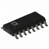
AD7888ARZ Analog Devices Inc, AD7888ARZ Datasheet

AD7888ARZ
Specifications of AD7888ARZ
Available stocks
Related parts for AD7888ARZ
AD7888ARZ Summary of contents
Page 1
GENERAL DESCRIPTION The AD7888 is a high speed, low power, 12-bit ADC that oper- ates from a single 2 5.25 V power supply. The AD7888 is capable of a 125 kSPS throughput rate. The input track-and- hold ...
Page 2
AD7888–SPECIFICATIONS otherwise noted MHz ( 5.25 V); T SCLK DD Parameter DYNAMIC PERFORMANCE 2, 3 Signal to Noise + Distortion Ratio (SNR Total Harmonic Distortion (THD) 2 Peak Harmonic or Spurious ...
Page 3
Parameter POWER REQUIREMENTS Normal Mode (Static) Normal Mode (Operational) Using Standby Mode Using Shutdown Mode 6 Standby Mode 6 Shutdown Mode Normal-Mode Power Dissipation Shutdown Power Dissipation Standby Power Dissipation NOTES 1 Temperature ranges as ...
Page 4
AD7888 1 TIMING SPECIFICATIONS Limit at T (A, B Versions) Parameter 4. 5. SCLK t 14.5 t CONVERT SCLK t 1.5 t ACQ SCLK ...
Page 5
Pin No. Mnemonic Function CS 1 Chip Select. Active low logic input. This input provides the dual function of initiating conversions on the AD7888 and also frames the serial data transfer. 2 REF IN/REF OUT Reference Input/Output. The on-chip reference ...
Page 6
AD7888 TERMINOLOGY Integral Nonlinearity This is the maximum deviation from a straight line passing through the endpoints of the ADC transfer function. The end- points of the transfer function are zero scale, a point 1/2 LSB below the first code ...
Page 7
CONTROL REGISTER The Control Register on the AD7888 is an 8-bit, write-only register. Data is loaded from the DIN pin of the AD7888 on the rising edge of SCLK. The data is transferred on the DIN line at the same ...
Page 8
AD7888 Figure 4 shows the typical power supply rejection ratio vs. frequency for the part. The power supply rejection ratio is defined as the ratio of the power in the ADC output at frequency f to the power of a ...
Page 9
TYPICAL CONNECTION DIAGRAM Figure 8 shows a typical connection diagram for the AD7888. Both AGND pins are connected to the analog ground plane of the system connected to a well decoupled V REF provide an analog input range ...
Page 10
AD7888 order to obtain optimum performance from the device it is advised to disable the internal reference by setting the REF bit in the Control Register when an external reference is applied. When the internal reference is disabled, SW1 in ...
Page 11
CS SCLK DOUT DIN MODES OF OPERATION The AD7888 has a number of different modes of operation. These are designed to provide flexible power management options. These options can be chosen to optimize the power dissipation/throughput rate ratio for differing ...
Page 12
AD7888 THE PART ENTERS SHUTDOWN AT THE END OF CONVERSION AS PM1 = 1 AND PM0 = SCLK 4 LEADING ZEROES DOUT + CONVERSION RESULT DIN DATA IN CONTROL REGISTER DATA IS LOADED ON THE FIRST ...
Page 13
SERIAL INTERFACE Figure 16 shows the detailed timing diagram for serial interfac- ing to the AD7888. The serial clock provides the conversion clock and also controls the transfer of information to and from the AD7888 during conversion. CS initiates the ...
Page 14
AD7888 MICROPROCESSOR INTERFACING The serial interface on the AD7888 allows the part to be directly connected to a range of many different microprocessors. This section explains how to interface the AD7888 with some of the more common microcontroller and DSP ...
Page 15
AD7888 to MC68HC11 The Serial Peripheral Interface (SPI) on the MC68HC11 is configured for Master Mode (MSTR = 1), Clock Polarity Bit (CPOL and the Clock Phase Bit (CPHA The SPI is configured by writing to ...
Page 16
AD7888 OUTLINE DIMENSIONS 4.00 (0.1575) 3.80 (0.1496) 0.25 (0.0098) 0.10 (0.0039) COPLANARITY 0.10 CONTROLLING DIMENSIONS ARE IN MILLIMETERS; INCH DIMENSIONS (IN PARENTHESES) ARE ROUNDED-OFF MILLIMETER EQUIVALENTS FOR REFERENCE ONLY AND ARE NOT APPROPRIATE FOR USE IN DESIGN. 4.50 4.40 4.30 ...
Page 17
... AD7888ARU-REEL ±2 AD7888ARU-REEL7 ±2 AD7888ARUZ ±2 AD7888ARUZ-REEL ±2 AD7888ARUZ-REEL7 ±2 AD7888ARZ ±2 AD7888ARZ-REEL ±2 AD7888ARZ-REEL7 ±2 AD7888BR-REEL ±1 AD7888BR-REEL7 ±1 AD7888BRZ ±1 3 EVAL-AD7888CB RoHS Compliant Part. 2 Linearity error here refers to integral linearity error. 3 This can be used as a standalone evaluation board or in conjunction with the EVAL-CONTROL BOARD for evaluation/demonstration purposes. ...


