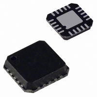
AD7689BCPZ Analog Devices Inc, AD7689BCPZ Datasheet - Page 15

AD7689BCPZ
Manufacturer Part Number
AD7689BCPZ
Description
IC ADC 16BIT 250KSPS 8CH 20LFCSP
Manufacturer
Analog Devices Inc
Series
PulSAR®r
Datasheet
1.AD7689ACPZ.pdf
(32 pages)
Specifications of AD7689BCPZ
Data Interface
DSP, MICROWIRE™, QSPI™, Serial, SPI™
Number Of Bits
16
Sampling Rate (per Second)
250k
Number Of Converters
1
Power Dissipation (max)
21mW
Voltage Supply Source
Single Supply
Operating Temperature
-40°C ~ 85°C
Mounting Type
Surface Mount
Package / Case
20-VFQFN, CSP Exposed Pad
Resolution (bits)
16bit
Sampling Rate
250kSPS
Input Channel Type
Differential
Supply Voltage Range - Analog
2.3V To 5.5V
Supply Voltage Range - Digital
1.8V To 5.5V
Lead Free Status / RoHS Status
Lead free / RoHS Compliant
Available stocks
Company
Part Number
Manufacturer
Quantity
Price
Company:
Part Number:
AD7689BCPZ
Manufacturer:
ADI
Quantity:
153
Company:
Part Number:
AD7689BCPZRL7
Manufacturer:
FUJI
Quantity:
150
Part Number:
AD7689BCPZRL7
Manufacturer:
ADI/亚德诺
Quantity:
20 000
THEORY OF OPERATION
OVERVIEW
The AD7682/AD7689 are 4-channel/8-channel, 16-bit, charge
redistribution successive approximation register (SAR) analog-
to-digital converters (ADCs). These devices are capable of
converting 250,000 samples per second (250 kSPS) and power
down between conversions. For example, when operating with
an external reference at 1 kSPS, they consume 17 μW typically,
ideal for battery-powered applications.
The AD7682/AD7689 contain all of the components for use in a
multichannel, low power data acquisition system, including
•
•
•
•
•
•
These components are configured through an SPI-compatible,
14-bit register. Conversion results, also SPI compatible, can be
read after or during conversions with the option for reading
back the configuration associated with the conversion.
The AD7682/AD7689 provide the user with an on-chip track-
and-hold and do not exhibit pipeline delay or latency.
The AD7682/AD7689 are specified from 2.3 V to 5.5 V and can
be interfaced to any 1.8 V to 5 V digital logic family. They are
housed in a 20-lead, 4 mm × 4 mm LFCSP that combines space
savings and allows flexible configurations. They are pin-for-pin
compatible with the 16-bit
16-bit SAR ADC with no missing codes
4-channel/8-channel, low crosstalk multiplexer
Internal low drift reference and buffer
Temperature sensor
Selectable one-pole filter
Channel sequencer
INx– OR
COM
INx+
GND
REF
AD7699
and 14-bit AD7949.
32,768C
32,768C
16,384C
16,384C
MSB
MSB
Figure 24. ADC Simplified Schematic
4C
4C
Rev. B | Page 15 of 32
2C
2C
CONVERTER OPERATION
The AD7682/AD7689 are successive approximation ADCs
based on a charge redistribution DAC. Figure 24 shows the
simplified schematic of the ADC. The capacitive DAC consists
of two identical arrays of 16 binary-weighted capacitors, which
are connected to the two comparator inputs.
During the acquisition phase, terminals of the array tied to the
comparator input are connected to GND via SW+ and SW−. All
independent switches are connected to the analog inputs.
Thus, the capacitor arrays are used as sampling capacitors and
acquire the analog signal on the INx+ and INx− (or COM)
inputs. When the acquisition phase is complete and the CNV
input goes high, a conversion phase is initiated. When the
conversion phase begins, SW+ and SW− are opened first. The
two capacitor arrays are then disconnected from the inputs and
connected to the GND input. Therefore, the differential voltage
between the INx+ and INx− (or COM) inputs captured at the
end of the acquisition phase is applied to the comparator inputs,
causing the comparator to become unbalanced. By switching
each element of the capacitor array between GND and REF, the
comparator input varies by binary-weighted voltage steps
(V
switches, starting with the MSB, to bring the comparator back
into a balanced condition. After the completion of this process,
the part returns to the acquisition phase, and the control logic
generates the ADC output code and a busy signal indicator.
Because the AD7682/AD7689 have an on-board conversion
clock, the serial clock, SCK, is not required for the conversion
process.
C
C
REF
/2, V
C
C
REF
LSB
LSB
/4, ... V
SW+
SW–
REF
COMP
/32,768). The control logic toggles these
SWITCHES CONTROL
CONTROL
LOGIC
CNV
AD7682/AD7689
BUSY
OUTPUT CODE


