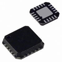
AD7689BCPZ Analog Devices Inc, AD7689BCPZ Datasheet - Page 27

AD7689BCPZ
Manufacturer Part Number
AD7689BCPZ
Description
IC ADC 16BIT 250KSPS 8CH 20LFCSP
Manufacturer
Analog Devices Inc
Series
PulSAR®r
Datasheet
1.AD7689ACPZ.pdf
(32 pages)
Specifications of AD7689BCPZ
Data Interface
DSP, MICROWIRE™, QSPI™, Serial, SPI™
Number Of Bits
16
Sampling Rate (per Second)
250k
Number Of Converters
1
Power Dissipation (max)
21mW
Voltage Supply Source
Single Supply
Operating Temperature
-40°C ~ 85°C
Mounting Type
Surface Mount
Package / Case
20-VFQFN, CSP Exposed Pad
Resolution (bits)
16bit
Sampling Rate
250kSPS
Input Channel Type
Differential
Supply Voltage Range - Analog
2.3V To 5.5V
Supply Voltage Range - Digital
1.8V To 5.5V
Lead Free Status / RoHS Status
Lead free / RoHS Compliant
Available stocks
Company
Part Number
Manufacturer
Quantity
Price
Company:
Part Number:
AD7689BCPZ
Manufacturer:
ADI
Quantity:
153
Company:
Part Number:
AD7689BCPZRL7
Manufacturer:
FUJI
Quantity:
150
Part Number:
AD7689BCPZRL7
Manufacturer:
ADI/亚德诺
Quantity:
20 000
CHANNEL SEQUENCER
The AD7682/AD7689 include a channel sequencer useful for
scanning channels in a repeated fashion. Channels are scanned
as singles or pairs, with or without the temperature sensor, after
the last channel is sequenced.
The sequencer starts with IN0 and finishes with IN[7:0] set in
CFG[9:7]. For paired channels, the channels are paired depend-
ing on the last channel set in CFG[9:7]. Note that in sequencer
mode, the channels are always paired with the positive input on
the even channels (IN0, IN2, IN4, IN6), and with the negative
input on the odd channels (IN1, IN3, IN5, IN7). For example,
setting CFG[9:7] = 110 or 111 scans all pairs with the positive
inputs dedicated to IN0, IN2, IN4, and IN6.
CFG[2:1] are used to enable the sequencer. After the CFG
register is updated, DIN must be held low while reading data
out for Bit 13, or the CFG register begins updating again.
Note that while operating in a sequence, some bits of the CFG
register can be changed. However, if changing CFG[11] (paired
or single channel) or CFG[9:7] (last channel in sequence), the
sequence reinitializes and converts IN0 (or IN0/IN1 pairs) after
the CFG register is updated.
Figure 39 details the timing for all three modes without a busy
indicator. Refer to the General Timing Without a Busy Indicator
section and the Read/Write Spanning Conversion Without a
RDC
RAC
RSC
NOTES
1. CNV MUST BE HIGH PRIOR TO THE END OF CONVERSION (EOC) TO AVOID THE BUSY INDICATOR.
2. A TOTAL OF 16 SCK FALLING EDGES ARE REQUIRED TO RETURN SDO TO HIGH-Z. IF CFG READBACK IS ENABLED,
PHASE
A TOTAL OF 30 SCK FALLING EDGES IS REQUIRED TO RETURN SDO TO HIGH-Z.
SDO
SCK
SDO
CNV
CNV
SDO
CNV
SCK
SCK
DIN
DIN
DIN
POWER
UP
MSB
XXX
(n – 2) UNDEFINED
1
CONVERSION
DATA (n – 3)
XXX
t
XXX
CONV
16
2
t
CYC
EOC
NOTE 1
(n – 1) UNDEFINED
ACQUISITION
1
1
DATA (n – 2)
DATA (n – 2)
CFG (n)
Figure 39. General Channel Sequencer Timing Without a Busy Indicator
CFG (n)
NOTE 2
XXX
XXX
16
n
SOC
n + 1
(n – 1) UNDEFINED
DATA (n – 2)
CONVERSION
1
CFG (n)
DATA (n – 2)
NOTE 2
t
DATA
CFG (n)
XXX
NOTE 2
XXX
16
16
Rev. B | Page 27 of 32
EOC
ACQUISITION
1
1
DATA (n – 1)
DATA (n – 1)
(n), IN0
XXX
XXX
MSB
XXX
16
n
Busy Indicator section for more details. The sequencer can also
be used with the busy indicator and details for these timings can
be found in the General Timing with a Busy Indicator section
and the Read/Write Spanning Conversion with a Busy Indicator
section.
For sequencer operation, the CFG register should be set during
the (n − 1) phase after power-up. On phase (n), the sequencer
setting takes place and acquires IN0. The first valid conversion
result is available at phase (n + 1). After the last channel set in
CFG[9:7] is converted, the internal temperature sensor data is
output (if enabled), followed by acquisition of IN0.
Examples
With all channels configured for unipolar mode to GND,
including the internal temperature sensor, the sequence scans in
the following order:
IN0, IN1, IN2, IN3, IN4, IN5, IN6, IN7, TEMP, IN0, IN1, IN2, …
For paired channels with the internal temperature sensor
enabled, the sequencer scans in the following order:
IN0, IN2, IN4, IN6, TEMP, IN0, …
Note that IN1, IN3, IN5, and IN7 are referenced to a GND
sense or V
n + 1
DATA (n – 1)
1
CONVERSION
DATA (n – 1)
XXX
(n), IN0
XXX
REF
16
16
/2, as detailed in the Input Configurations section.
EOC
ACQUISITION
1
1
(n + 1), IN1
DATA IN0
DATA IN0
16
MSB
n
IN0
n + 1
CONVERSION
1
DATA IN0
(n + 1), IN1
DATA IN0
AD7682/AD7689
16
16
EOC
ACQUISITION
1
1
(n + 2), IN2
DATA IN1
DATA IN1
n
MSB
IN1


