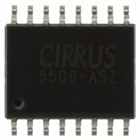
CS5509-ASZ Cirrus Logic Inc, CS5509-ASZ Datasheet - Page 10

CS5509-ASZ
Manufacturer Part Number
CS5509-ASZ
Description
IC ADC 16BIT SGNL SUPP 16-SOIC
Manufacturer
Cirrus Logic Inc
Datasheet
1.CS5509-ASZ.pdf
(24 pages)
Specifications of CS5509-ASZ
Number Of Converters
1
Package / Case
16-SOIC (0.300", 7.50mm Width)
Number Of Bits
16
Sampling Rate (per Second)
200
Data Interface
Serial
Power Dissipation (max)
2.25mW
Voltage Supply Source
Analog and Digital
Operating Temperature
-40°C ~ 85°C
Mounting Type
Surface Mount
Number Of Adc Inputs
1
Architecture
Delta-Sigma
Conversion Rate
20 SPs
Resolution
16 bit
Input Type
Voltage
Interface Type
Serial
Voltage Reference
1.2 V
Supply Voltage (max)
5 V
Supply Voltage (min)
3.3 V
Maximum Power Dissipation
2.25 mW
Maximum Operating Temperature
+ 85 C
Mounting Style
SMD/SMT
Input Voltage
3.3 V to 5 V
Minimum Operating Temperature
- 40 C
Lead Free Status / RoHS Status
Lead free / RoHS Compliant
Lead Free Status / RoHS Status
Lead free / RoHS Compliant, Lead free / RoHS Compliant
Other names
598-1100-5
Available stocks
Company
Part Number
Manufacturer
Quantity
Price
Company:
Part Number:
CS5509-ASZ
Manufacturer:
CIRRUS
Quantity:
44
Part Number:
CS5509-ASZ
Manufacturer:
CIRRUS
Quantity:
20 000
GENERAL DESCRIPTION
The CS5509 is a low power, 16-bit, monolithic
CMOS A/D converter designed specifically for
measurement of dc signals. The CS5509 includes a
delta-sigma charge-balance converter, a voltage
reference, a calibration microcontroller with
SRAM, a digital filter and a serial interface.
The CS5509 is optimized to operate from a 32.768
kHz crystal but can be driven by an external clock
whose frequency is between 30kHz and 330kHz.
When the digital filter is operated with a 32.768
kHz clock, the filter has zeros precisely at 50 and
60 Hz line frequencies and multiples thereof.
The CS5509 uses a "start convert" command to
start a convolution cycle on the digital filter. Once
the filter cycle is completed, the output port is up-
dated.When operated with a 32.768kHz clock the
ADC converts and updates its output port at 20
samples/sec.The output port operates in a synchro-
nous externally-clocked interface format.
THEORY OF OPERATION
Basic Converter Operation
The CS5509 A/D converter has three operating
states. These are stand-by, calibration, and conver-
sion. When power is first applied, an internal pow-
er-on reset delay of about 10 ms resets all of the
logic in the device. The oscillator must then begin
oscillating before the device can be considered
functional. After the power-on reset is applied, the
device enters the wake-up period for 1800 clock
cycles after clock is present. This allows the delta-
sigma modulator and other circuitry (which are op-
erating with very low currents) to reach a stable
bias condition prior to entering into either the cali-
bration or conversion states. During the 1800 cycle
wake-up period, the device can accept an input
command. Execution of this command will not oc-
cur until the complete wake-up period elapses. If
no command is given, the device enters the standby
state.
10
Calibration
After the initial application of power, the CS5509
must enter the calibration state prior to performing
accurate conversions. During calibration, the chip
executes a two-step process. The device first per-
forms an offset calibration and then follows this
with a gain calibration. The two calibration steps
determine the zero reference point and the full scale
reference point of the converter's transfer function.
From these points it calibrates the zero point and a
gain slope to be used to properly scale the output
digital codes when doing conversions.
The calibration state is entered whenever the CAL
and CONV pins are high at the same time. The state
of the CAL and CONV pins at power-on are recog-
nized as commands, but will not be executed until
the end of the 1800 clock cycle wake-up period.
If CAL and CONV become active (high) during the
1800 clock cycle wake-up time, the converter will
wait until the wake-up period elapses before exe-
cuting the calibration. If the wake-up time has
elapsed, the converter will be in the standby mode
waiting for instruction and will enter the calibration
cycle immediately if CAL and CONV become ac-
tive. The calibration lasts for 3246 clock cycles.
Calibration coefficients are then retained in the
SRAM (static RAM) for use during conversion.
The state of BP/UP is ignored during calibration
but should remain stable throughout the calibration
period to minimize noise.
When conversions are performed in unipolar mode
or in bipolar mode, the converter uses the same cal-
ibration factors to compute the digital output code.
The only difference is that in bipolar mode the on-
chip microcontroller offsets the computed output
word by a code value of 8000H. This means that the
bipolar measurement range is not calibrated from
full scale positive to full scale negative. Instead it is
calibrated from the bipolar zero scale point to full
scale positive. The slope factor is then extended be-
low bipolar zero to accommodate the negative in-
CS5509
DS125F3


