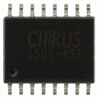
CS5509-ASZ Cirrus Logic Inc, CS5509-ASZ Datasheet - Page 19

CS5509-ASZ
Manufacturer Part Number
CS5509-ASZ
Description
IC ADC 16BIT SGNL SUPP 16-SOIC
Manufacturer
Cirrus Logic Inc
Datasheet
1.CS5509-ASZ.pdf
(24 pages)
Specifications of CS5509-ASZ
Number Of Converters
1
Package / Case
16-SOIC (0.300", 7.50mm Width)
Number Of Bits
16
Sampling Rate (per Second)
200
Data Interface
Serial
Power Dissipation (max)
2.25mW
Voltage Supply Source
Analog and Digital
Operating Temperature
-40°C ~ 85°C
Mounting Type
Surface Mount
Number Of Adc Inputs
1
Architecture
Delta-Sigma
Conversion Rate
20 SPs
Resolution
16 bit
Input Type
Voltage
Interface Type
Serial
Voltage Reference
1.2 V
Supply Voltage (max)
5 V
Supply Voltage (min)
3.3 V
Maximum Power Dissipation
2.25 mW
Maximum Operating Temperature
+ 85 C
Mounting Style
SMD/SMT
Input Voltage
3.3 V to 5 V
Minimum Operating Temperature
- 40 C
Lead Free Status / RoHS Status
Lead free / RoHS Compliant
Lead Free Status / RoHS Status
Lead free / RoHS Compliant, Lead free / RoHS Compliant
Other names
598-1100-5
Available stocks
Company
Part Number
Manufacturer
Quantity
Price
Company:
Part Number:
CS5509-ASZ
Manufacturer:
CIRRUS
Quantity:
44
Part Number:
CS5509-ASZ
Manufacturer:
CIRRUS
Quantity:
20 000
PIN DESCRIPTIONS*
* Pinout applies to both PDIP and SOIC
Clock Generator
XIN; XOUT - Crystal In; Crystal Out, Pins 4, 5.
Serial Output I/O
CS - Chip Select, Pin 1.
DRDY - Data Ready, Pin 16.
SDATA - Serial Data Output, Pin 15.
SCLK - Serial Clock Input, Pin 14.
DS125F3
DIFFERENTIAL ANALOG INPUT
DIFFERENTIAL ANALOG INPUT
A gate inside the chip is connected to these pins and can be used with a crystal to provide the
master clock for the device. Alternatively, an external (CMOS compatible) clock can be
supplied into the XIN pin to provide the master clock for the device. Loss of clock will put the
device into a lower powered state (approximately 70% power reduction).
This input allows an external device to access the serial port.
Data Ready goes low at the end of a digital filter convolution cycle to indicate that a new
output word has been placed into the serial port. DRDY will return high after all data bits are
shifted out of the serial port or two master clock cycles before new data becomes available if
the CS pin is inactive (high).
SDATA is the output pin of the serial output port. Data from this pin will be output at a rate
determined by SCLK. Data is output MSB first and advances to the next data bit on the falling
edges of SCLK. SDATA will be in a high impedance state when not transmitting data.
A clock signal on this pin determines the output rate of the data from the SDATA pin. This pin
must not be allowed to float.
BIPOLAR / UNIPOLAR
CRYSTAL OUT
CHIP SELECT
CRYSTAL IN
CALIBRATE
CONVERT
BP/UP
CONV
XOUT
AIN+
CAL
AIN-
XIN
CS
1
2
3
4
5
6
7
8
16
15
14
13
12
11
10
9
DRDY
SDATA
SCLK
VD+
GND
VA+
VREF-
VREF+
DATA READY
SERIAL DATA OUTPUT
SERIAL CLOCK INPUT
POSITIVE DIGITAL POWER
GROUND
POSITIVE ANALOG POWER
VOLTAGE REFERENCE INPUT
VOLTAGE REFERENCE INPUT
CS5509
19


