CS5509-ASZ Cirrus Logic Inc, CS5509-ASZ Datasheet - Page 9
CS5509-ASZ
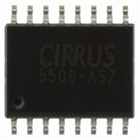
Manufacturer Part Number
CS5509-ASZ
Description
IC ADC 16BIT SGNL SUPP 16-SOIC
Manufacturer
Cirrus Logic Inc
Datasheet
1.CS5509-ASZ.pdf
(24 pages)
Specifications of CS5509-ASZ
Number Of Converters
1
Package / Case
16-SOIC (0.300", 7.50mm Width)
Number Of Bits
16
Sampling Rate (per Second)
200
Data Interface
Serial
Power Dissipation (max)
2.25mW
Voltage Supply Source
Analog and Digital
Operating Temperature
-40°C ~ 85°C
Mounting Type
Surface Mount
Number Of Adc Inputs
1
Architecture
Delta-Sigma
Conversion Rate
20 SPs
Resolution
16 bit
Input Type
Voltage
Interface Type
Serial
Voltage Reference
1.2 V
Supply Voltage (max)
5 V
Supply Voltage (min)
3.3 V
Maximum Power Dissipation
2.25 mW
Maximum Operating Temperature
+ 85 C
Mounting Style
SMD/SMT
Input Voltage
3.3 V to 5 V
Minimum Operating Temperature
- 40 C
Lead Free Status / RoHS Status
Lead free / RoHS Compliant
Lead Free Status / RoHS Status
Lead free / RoHS Compliant, Lead free / RoHS Compliant
Other names
598-1100-5
Available stocks
Company
Part Number
Manufacturer
Quantity
Price
Company:

Part Number:
CS5509-ASZ
Manufacturer:
CIRRUS
Quantity:
44
Part Number:
CS5509-ASZ
Manufacturer:
CIRRUS
Quantity:
20 000


RECOMMENDED OPERATING CONDITIONS
Notes: 19. All voltages with respect to ground.
ABSOLUTE MAXIMUM RATINGS*
Notes: 21. No pin should go more positive than (VA+) + 0.3 V.
*WARNING:Operation at or beyond these limits may result in permanent damage to the device.
DS125F3
DC Power Supplies
Analog Reference Voltage
Analog Input Voltage
DC Power Supplies
Input Current, Any Pin Except Supplies
Output Current
Power Dissipation (Total)
Analog Input Voltage
Digital Input Voltage
Ambient Operating Temperature
Storage Temperature
20. The CS5509 can be operated with a reference voltage as low as 100 mV; but with a corresponding
22. VD+ must always be less than (VA+) + 0.3 V, and can never exceed +6.0 V.
23. Applies to all pins including continuous overvoltage conditions at the analog input (AIN) pin.
24. Transient currents of up to 100 mA will not cause SCR latch-up. Maximum input current for a power
25. Total power dissipation, including all input currents and output currents.
reduction in noise-free resolution. The common mode voltage of the voltage reference may be any value
as long as +VREF and -VREF remain inside the supply values of VA+ and GND.
supply pin is ± 50 mA.
Normal operation is not guaranteed at these extremes.
Parameter
Positive Analog
Positive Digital
Parameter
Ground
Positive Digital
Positive Analog
(Note 20)
Unipolar
(Note 6)
Bipolar
(VREF+) -
AIN and VREF pins
(VREF-)
Symbol
(Notes 23 and 24)
VAIN
VAIN
VD+
VA+
(Note 21)
(Note 22)
(Note 25)
-((VREF+) - (VREF-))
Symbol
3.15
4.75
Min
1.0
0
GND
V
V
VD+
VA+
T
I
T
I
out
IND
INA
stg
in
A
(DGND = 0V) (Note 19)
Min
-0.3
-0.3
-0.3
-0.3
-0.3
-40
-65
-
-
-
Typ
5.0
5.0
2.5
-
-
(VREF+) - (VREF-)
(VREF+) - (VREF-)
Typ
-
-
-
-
-
-
-
-
-
-
Max
3.6
5.5
5.5
(VD+)+0.3
(VA+)+0.3
(VD+)-0.3
Max
500
±10
±25
150
6.0
6.0
85
CS5509
Unit
mW
Unit
mA
mA
°C
°C
V
V
V
V
V
V
V
V
V
V
9
Related parts for CS5509-ASZ
Image
Part Number
Description
Manufacturer
Datasheet
Request
R

Part Number:
Description:
A/D Converter (A-D) IC
Manufacturer:
Cirrus Logic Inc
Datasheet:
Part Number:
Description:
IC Single-Supply 16-Bit ADC
Manufacturer:
Cirrus Logic Inc
Datasheet:

Part Number:
Description:
Development Kit
Manufacturer:
Cirrus Logic Inc
Datasheet:
Part Number:
Description:
Development Kit
Manufacturer:
Cirrus Logic Inc
Datasheet:


Part Number:
Description:
High-efficiency PFC + Fluorescent Lamp Driver Reference Design
Manufacturer:
Cirrus Logic Inc
Datasheet:
Part Number:
Description:
Development Kit
Manufacturer:
Cirrus Logic Inc
Datasheet:
Part Number:
Description:
Development Kit
Manufacturer:
Cirrus Logic Inc
Datasheet:

Part Number:
Description:
Development Kit
Manufacturer:
Cirrus Logic Inc
Datasheet:
Part Number:
Description:
Development Kit
Manufacturer:
Cirrus Logic Inc
Datasheet:
Part Number:
Description:
Development Kit
Manufacturer:
Cirrus Logic Inc
Datasheet:
Part Number:
Description:
Development Kit
Manufacturer:
Cirrus Logic Inc
Datasheet:

Part Number:
Description:
Ref Bd For Speakerbar MSA & DSP Products
Manufacturer:
Cirrus Logic Inc