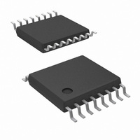
ADC78H89CIMT/NOPB National Semiconductor, ADC78H89CIMT/NOPB Datasheet

ADC78H89CIMT/NOPB
Specifications of ADC78H89CIMT/NOPB
*ADC78H89CIMT/NOPB
ADC78H89CIMT
Available stocks
Related parts for ADC78H89CIMT/NOPB
ADC78H89CIMT/NOPB Summary of contents
Page 1
... Connection Diagram Ordering Information Order Code ADC78H89CIMT ADC78H89CIMTX ADC78H89EVAL TRI-STATE ® trademark of National Semiconductor Corporation. MICROWIRE is a trademark of National Semiconductor Corporation. ™ QSPI ™ and SPI ™ are trademarks of Motorola, Inc. © 2005 National Semiconductor Corporation ...
Page 2
Block Diagram Pin Descriptions and Equivalent Circuits Pin No. Symbol ANALOG I AIN1 to AIN7 2 NC DIGITAL I/O 16 SCLK 15 DOUT 14 DIN 1 CS POWER SUPPLY ...
Page 3
... Absolute Maximum Ratings If Military/Aerospace specified devices are required, please contact the National Semiconductor Sales Office/ Distributors for availability and specifications. Analog Supply Voltage AV DD Digital Supply Voltage DV DD Voltage on Any Pin to GND Input Current at Any Pin (Note 3) Package Input Current (Note 3) Power Dissipation 25˚ ...
Page 4
ADC78H89 Converter Electrical Characteristics The following specifications apply for AV noted. Boldface limits apply for T A Symbol Parameter ANALOG INPUT CHARACTERISTICS V Input Range Leakage Current DCL C Input Capacitance INA DIGITAL INPUT CHARACTERISTICS V Input ...
Page 5
ADC78H89 Timing Specifications The following specifications apply for all other limits T A MIN MAX A Symbol Parameter t SCLK High to CS Fall Setup Time 1a t SCLK Low to CS Fall ...
Page 6
Timing Diagrams www.national.com FIGURE 1. ADC78H89 Operational Timing Diagram Timing Test Circuit ADC78H89 Serial Timing Diagram 6 20061651 20061608 20061606 ...
Page 7
Timing Diagrams (Continued) 20061650 SCLK and CS Timing Parameters 7 www.national.com ...
Page 8
Specification Definitions ACQUISITION TIME is the time required to acquire the input voltage. That is time required for the hold capacitor to charge up to the input voltage. APERTURE DELAY is the time between the fourth falling SCLK ...
Page 9
Typical Performance Characteristics kHz unless otherwise stated. DNL INL DNL vs. Supply T = +25˚ 500 KSPS SAMPLE 20061640 20061642 20061621 MHz 40.2 SCLK IN DNL 20061641 INL 20061643 INL vs. ...
Page 10
Typical Performance Characteristics kHz unless otherwise stated. (Continued) SNR vs. Supply ENOB vs. Supply THD vs. Input Frequency www.national.com T = +25˚ 500 KSPS SAMPLE 20061622 SNR vs. Input Frequency 20061633 ENOB vs. Input Frequency 20061624 ...
Page 11
Typical Performance Characteristics kHz unless otherwise stated. (Continued) Spectral Response Power Consumption vs. Throughput T = +25˚ 500 KSPS SAMPLE Spectral Response 20061630 20061644 MHz 40.2 SCLK IN 20061631 www.national.com ...
Page 12
Applications Information 1.0 USING THE ADC78H89 An operational timing diagram and a serial interface timing diagram for the ADC78H89 are shown in the Timing Dia- grams section chip select, which initiates conversions and frames the serial data transfers. ...
Page 13
Applications Information Bit 7 (MSB) Bit 6 DONTC DONTC Bit #: Symbol DONTC 5 ADD2 4 ADD1 3 ADD0 TABLE 2. Input Channel Selection ADD2 ADD1 ADD0 ...
Page 14
Applications Information 3.0 ADC78H89 TRANSFER FUNCTION The output format of the ADC89H89 is straight binary. Code transitions occur midway between successive integer LSB values. The LSB width for the ADC78H89 is AV The ideal transfer characteristic is shown in Figure ...
Page 15
Applications Information to sample AC signals, a band-pass or low-pass filter will reduce harmonics and noise, improving dynamic perfor- mance. 6.0 DIGITAL INPUTS AND OUTPUTS The ADC78H89’s digital inputs (SCLK, CS, and DIN) are limited by and cannot exceed the ...
Page 16
... BANNED SUBSTANCE COMPLIANCE National Semiconductor manufactures products and uses packing materials that meet the provisions of the Customer Products Stewardship Specification (CSP-9-111C2) and the Banned Substances and Materials of Interest Specification (CSP-9-111S2) and contain no ‘‘Banned Substances’’ as defined in CSP-9-111S2. ...


