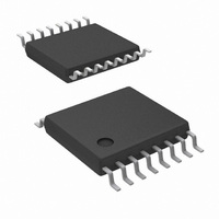
ADC78H89CIMT/NOPB National Semiconductor, ADC78H89CIMT/NOPB Datasheet - Page 15

ADC78H89CIMT/NOPB
Manufacturer Part Number
ADC78H89CIMT/NOPB
Description
IC ADC 12BIT 500KSPS 7CH 16TSSOP
Manufacturer
National Semiconductor
Series
PowerWise®r
Datasheet
1.ADC78H89CIMTNOPB.pdf
(16 pages)
Specifications of ADC78H89CIMT/NOPB
Number Of Bits
12
Sampling Rate (per Second)
500k
Data Interface
DSP, MICROWIRE™, QSPI™, Serial, SPI™
Number Of Converters
1
Power Dissipation (max)
8.3mW
Voltage Supply Source
Analog and Digital
Operating Temperature
-40°C ~ 85°C
Mounting Type
Surface Mount
Package / Case
16-TSSOP (0.173", 4.40mm Width)
Number Of Elements
1
Resolution
12Bit
Architecture
SAR
Sample Rate
500KSPS
Input Polarity
Unipolar
Input Type
Voltage
Rated Input Volt
5.25V
Differential Input
No
Power Supply Requirement
Analog and Digital
Single Supply Voltage (typ)
3.3/5V
Single Supply Voltage (min)
2.7V
Single Supply Voltage (max)
5.25V
Dual Supply Voltage (typ)
Not RequiredV
Dual Supply Voltage (min)
Not RequiredV
Dual Supply Voltage (max)
Not RequiredV
Differential Linearity Error
±1LSB
Integral Nonlinearity Error
±1LSB
Operating Temp Range
-40C to 85C
Operating Temperature Classification
Industrial
Mounting
Surface Mount
Pin Count
16
Package Type
TSSOP
Input Signal Type
Single-Ended
Lead Free Status / RoHS Status
Lead free / RoHS Compliant
Other names
*ADC78H89CIMT
*ADC78H89CIMT/NOPB
ADC78H89CIMT
*ADC78H89CIMT/NOPB
ADC78H89CIMT
Available stocks
Company
Part Number
Manufacturer
Quantity
Price
Company:
Part Number:
ADC78H89CIMT/NOPB
Manufacturer:
TI
Quantity:
3 100
Applications Information
to sample AC signals, a band-pass or low-pass filter will
reduce harmonics and noise, improving dynamic perfor-
mance.
6.0 DIGITAL INPUTS AND OUTPUTS
The ADC78H89’s digital inputs (SCLK, CS, and DIN) are
limited by and cannot exceed the analog supply voltage
AV
CS, and DIN may be asserted before DV
7.0 POWER SUPPLY CONSIDERATIONS
The ADC78H89 has two supplies, although they could both
have the same potential. There are two major power supply
concerns with this product. They are relative power supply
levels, including power-on sequencing, and the effect of
digital supply noise on the analog supply.
7.1 Power Management
The ADC78H89 is a dual-supply device. These two supplies
share ESD resources, and thus care must be exercised to
ensure that the power supplies are applied in the correct
sequence. To avoid turning on the ESD diodes, the digital
supply (DV
more than 300 mV. The ADC78H89’s analog power supply
must, therefore, be applied before (or concurrently with) the
digital power supply.
The ADC78H89 is fully powered-up whenever CS is low, and
fully powered-down whenever CS is high, with one excep-
tion: the ADC78H89 automatically enters power-down mode
between the 16th falling edge of a conversion and the 1st
falling edge of the subsequent conversion (see Figure 1).
The ADC78H89 can perform multiple conversions back to
back; each conversion requires 16 SCLK cycles. The
ADC78H89 will perform conversions continuously as long as
CS is held low.
The user may trade off throughput for power consumption by
simply performing fewer conversions per unit time. The
DD
. The digital input pins are not prone to latch-up; SCLK,
DD
) cannot exceed the analog supply (AV
DD
without any risk.
(Continued)
DD
) by
15
Power Consumption vs. Sample Rate curve in the Typical
Performance Curves section shows the typical power con-
sumption of the ADC78H89 versus throughput. To calculate
the power consumption, simply multiply the fraction of time
spent in the normal mode by the normal mode power con-
sumption (8.3 mW with AV
and add the fraction of time spent in shutdown mode multi-
plied by the shutdown mode power dissipation (0.3 mW with
AV
7.2 Power Supply Noise Considerations
The charging of any output load capacitance requires cur-
rent from the digital supply, DV
quired from the supply to charge the output capacitance will
cause voltage variations on the digital supply. If these varia-
tions are large enough, they could cause degrade SNR and
SINAD performance of the ADC. Furthermore, if the analog
and digital supplies are tied directly together, the noise on
the digital supply will be coupled directly into the analog
supply, causing greater performance degradation than noise
on the digital supply. Furthermore, discharging the output
capacitance when the digital output goes from a logic high to
a logic low will dump current into the die substrate, which is
resistive. Load discharge currents will cause "ground
bounce" noise in the substrate that will degrade noise per-
formance if that current is large enough. The larger is the
output capacitance, the more current flows through the die
substrate and the greater is the noise coupled into the
analog channel, degrading noise performance.
The first solution is to decouple the analog and digital sup-
plies from each other, or use separate supplies for them, to
keep digital noise out of the analog supply. To keep noise out
of the digital supply, keep the output load capacitance as
small as practical. If the load capacitance is greater than 25
pF, use a 100 Ω series resistor at the ADC output, located as
close to the ADC output pin as practical. This will limit the
charge and discharge current of the output capacitance and
improve noise performance.
DD
= DV
DD
= +3.6V).
DD
= DV
DD
DD
. The current pulses re-
= +3.6V, for example),
www.national.com


