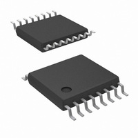
ADC78H89CIMT/NOPB National Semiconductor, ADC78H89CIMT/NOPB Datasheet - Page 4

ADC78H89CIMT/NOPB
Manufacturer Part Number
ADC78H89CIMT/NOPB
Description
IC ADC 12BIT 500KSPS 7CH 16TSSOP
Manufacturer
National Semiconductor
Series
PowerWise®r
Datasheet
1.ADC78H89CIMTNOPB.pdf
(16 pages)
Specifications of ADC78H89CIMT/NOPB
Number Of Bits
12
Sampling Rate (per Second)
500k
Data Interface
DSP, MICROWIRE™, QSPI™, Serial, SPI™
Number Of Converters
1
Power Dissipation (max)
8.3mW
Voltage Supply Source
Analog and Digital
Operating Temperature
-40°C ~ 85°C
Mounting Type
Surface Mount
Package / Case
16-TSSOP (0.173", 4.40mm Width)
Number Of Elements
1
Resolution
12Bit
Architecture
SAR
Sample Rate
500KSPS
Input Polarity
Unipolar
Input Type
Voltage
Rated Input Volt
5.25V
Differential Input
No
Power Supply Requirement
Analog and Digital
Single Supply Voltage (typ)
3.3/5V
Single Supply Voltage (min)
2.7V
Single Supply Voltage (max)
5.25V
Dual Supply Voltage (typ)
Not RequiredV
Dual Supply Voltage (min)
Not RequiredV
Dual Supply Voltage (max)
Not RequiredV
Differential Linearity Error
±1LSB
Integral Nonlinearity Error
±1LSB
Operating Temp Range
-40C to 85C
Operating Temperature Classification
Industrial
Mounting
Surface Mount
Pin Count
16
Package Type
TSSOP
Input Signal Type
Single-Ended
Lead Free Status / RoHS Status
Lead free / RoHS Compliant
Other names
*ADC78H89CIMT
*ADC78H89CIMT/NOPB
ADC78H89CIMT
*ADC78H89CIMT/NOPB
ADC78H89CIMT
Available stocks
Company
Part Number
Manufacturer
Quantity
Price
Company:
Part Number:
ADC78H89CIMT/NOPB
Manufacturer:
TI
Quantity:
3 100
www.national.com
ANALOG INPUT CHARACTERISTICS
V
I
C
DIGITAL INPUT CHARACTERISTICS
V
V
I
C
DIGITAL OUTPUT CHARACTERISTICS
V
V
I
I
C
POWER SUPPLY CHARACTERISTICS (C
AV
DV
I
P
AC ELECTRICAL CHARACTERISTICS
f
f
t
DC
t
f
t
DCL
IN
OZH
OZL
DD
SCLK
S
CONV
ACQ
RATE
AD
Symbol
ADC78H89 Converter Electrical Characteristics
IN
INA
IH
IL
IND
OH
OL
OUT
D
The following specifications apply for AV
noted. Boldface limits apply for T
DD
DD
,
,
Input Range
DC Leakage Current
Input Capacitance
Input High Voltage
Input Low Voltage
Input Current
Input Capacitance
Output High Voltage
Output Low Voltage
TRI-STATE Leakage Current
TRI-STATE Output Capacitance
Output Coding
Analog and Digital Supply Voltages
Total Supply Current, Normal Mode
(Operational, CS low)
Total Supply Current, Shutdown (CS
high)
Power Consumption, Normal Mode
(Operational, CS low)
Power Consumption, Shutdown (CS
high)
Maximum Clock Frequency
Minimum Clock Frequency
Maximum Sample Rate
Conversion Time
Duty Cycle
Track/Hold Acquisition Time
Throughput Time
Throughput Rate
Aperture Delay
Parameter
A
= T
DD
MIN
L
= 10 pF)
= DV
to T
In Track Mode
In Hold Mode
DV
DV
DV
V
I
DV
I
AV
AV
f
AV
f
AV
f
AV
f
AV
AV
AV
AV
Full-Scale Step Input
Conversion Time + Acquisition Time
MAX
DD
SOURCE
SINK
SAMPLE
SAMPLE
SAMPLE
SAMPLE
IN
DD
DD
DD
DD
DD
DD
DD
DD
DD
DD
DD
DD
DD
= +2.7V to 5.25V, f
= 0V or DV
: all other limits T
= 200 µA
≥ DV
= DV
= DV
= DV
= DV
= DV
= DV
= DV
= DV
= +4.75Vto +5.25V
= +2.7V to +3.6V
= +2.7V to +5.25V
= +2.7V to +5.25V
= 0 KSPS
= 500 KSPS, f
= 500 KSPS, f
= 0 KSPS
= 200 µA,
DD
DD
DD
DD
DD
DD
DD
DD
DD
Conditions
4
= +4.75V to +5.25V,
= +2.7V to +3.6V,
= +4.75V to +5.25V,
= +2.7V to +3.6V,
= +4.75V to +5.25V
= +2.7V to +3.6V
= +4.75V to +5.25V
= +2.7V to +3.6V
DD
A
SCLK
IN
IN
= 25˚C.
= 40 kHz
= 40 kHz
= 8 MHz, f
(Note 8) (Continued)
SAMPLE
0 to AV
Typical
±
1.65
0.5
0.1
0.1
8.3
1.5
0.5
0.3
0.01
33
50
13
50
3
2
2
4
= 500 KSPS unless otherwise
DD
Straight (Natural) Binary
DV
Limits
DD
5.25
500
500
2.4
2.1
0.8
0.4
2.7
2.3
2.3
8.3
±
±
12
13
40
60
16
1
4
4
8
3
1
1
−0.5
SCLK cycles
SCLK cycles
SCLK cycles
KSPS (min)
KSPS (min)
MHz (max)
mW (max)
mW (max)
mA (max)
mA (max)
µA (max)
µA (max)
µA (max)
pF (max)
pF (max)
% (max)
(Note 7)
V (max)
V (max)
V (max)
% (min)
V (min)
V (min)
V (min)
V (min)
Units
kHz
µW
µW
pF
pF
µA
µA
ns
V


