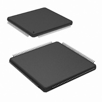
ADC083000CIYB/NOPB National Semiconductor, ADC083000CIYB/NOPB Datasheet - Page 11

ADC083000CIYB/NOPB
Manufacturer Part Number
ADC083000CIYB/NOPB
Description
IC ADC 8BIT 3GSPS LP 128-LQFP
Manufacturer
National Semiconductor
Series
PowerWise®r
Datasheet
1.ADC083000CIYBNOPB.pdf
(40 pages)
Specifications of ADC083000CIYB/NOPB
Number Of Bits
8
Sampling Rate (per Second)
3G
Data Interface
Serial
Number Of Converters
2
Power Dissipation (max)
2.3W
Voltage Supply Source
Single Supply
Operating Temperature
-40°C ~ 85°C
Mounting Type
Surface Mount
Package / Case
128-LQFP Exposed Pad
Lead Free Status / RoHS Status
Lead free / RoHS Compliant
Other names
*ADC083000CIYB
*ADC083000CIYB/NOPB
ADC083000CIYB
*ADC083000CIYB/NOPB
ADC083000CIYB
Available stocks
Company
Part Number
Manufacturer
Quantity
Price
Company:
Part Number:
ADC083000CIYB/NOPB
Manufacturer:
IPS
Quantity:
2 300
Part Number:
ADC083000CIYB/NOPB
Manufacturer:
TI/德州仪器
Quantity:
20 000
TEMPERATURE DIODE CHARACTERISTICS
ΔV
LVDS INPUT CHARACTERISTICS
V
I
C
LVDS OUTPUT CHARACTERISTICS
V
Δ V
V
V
Δ V
I
Z
LVCMOS INPUT CHARACTERISTICS
V
V
C
LVCMOS OUTPUT CHARACTERISTICS
V
V
POWER SUPPLY CHARACTERISTICS
I
I
P
PSRR1
PSRR2
I
OS
A
DR
O
ID
OD
OS
OS
IH
IL
OH
OL
D
IN
IN
Symbol
BE
O DIFF
OS
Temperature Diode Voltage
Differential Clock Input Level
Input Current
Input Capacitance (Notes 10, 11)
LVDS Differential Output Voltage
Change in LVDS Output Swing
Between Logic Levels
Output Offset Voltage,
see Figure 1
Output Offset Voltage,
see Figure 1
Output Offset Voltage Change
Between Logic Levels
Output Short Circuit Current
Differential Output Impedance
Logic High Input Voltage
Logic Low Input Voltage
Input Capacitance (Notes 11, 13) Each input to ground
CMOS H level output
CMOS L level output
Analog Supply Current
Output Driver Supply Current
Power Consumption
D.C. Power Supply Rejection
Ratio
A.C. Power Supply Rejection
Ratio
Parameter
192 µA vs. 12 µA,
T
192 µA vs. 12 µA,
T
Sine Wave Clock
Square Wave Clock
V
Differential
Each input to ground
Measured differentially, OutV = V
= Floating (Note 15)
Measured differentially, OutV = GND,
V
V
V
Output+ & Output- connected to 0.8V
(Note 12)
(Note 12)
I
I
PD = Low
PD = Low
PD = Low
PD = High
Change in offset with change in V
1.8V to 2.0V
248 MHz, 100mV
OH
OH
J
J
IN
BG
BG
BG
= 25°C
= 85°C
= 0 or V
= -400uA (Note 12)
= 400uA (Note 12)
= Floating (Note 15)
= Floating
= V
A
(Note 15)
IN
Conditions
= V
11
A
P-P
riding on V
A
A
A
, V
from
BG
(Note 8)
Typical
71.23
85.54
1150
0.02
1.65
0.15
680
520
800
100
734
300
0.6
0.6
1.5
1.2
1.9
±1
±1
±1
±4
25
70
50
0.85 x V
0.15 x V
(Note 8)
Limits
470
920
380
720
810
410
0.4
2.0
0.4
2.0
1.5
0.3
2.3
A
A
mV
mV
mV
mV
www.national.com
V
V
V
V
mA (max)
mA (max)
W (max)
(Limits)
V (max)
P-P
P-P
V (min)
P-P
P-P
Ohms
P-P
P-P
Units
P-P
P-P
mW
mV
mV
mV
mV
mV
mV
mA
µA
pF
pF
pF
dB
dB
V
V
(max)
(max)
(min)
(min)
(max)
(max)
(min)
(min)


