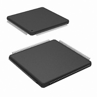
ADC083000CIYB/NOPB National Semiconductor, ADC083000CIYB/NOPB Datasheet - Page 33

ADC083000CIYB/NOPB
Manufacturer Part Number
ADC083000CIYB/NOPB
Description
IC ADC 8BIT 3GSPS LP 128-LQFP
Manufacturer
National Semiconductor
Series
PowerWise®r
Datasheet
1.ADC083000CIYBNOPB.pdf
(40 pages)
Specifications of ADC083000CIYB/NOPB
Number Of Bits
8
Sampling Rate (per Second)
3G
Data Interface
Serial
Number Of Converters
2
Power Dissipation (max)
2.3W
Voltage Supply Source
Single Supply
Operating Temperature
-40°C ~ 85°C
Mounting Type
Surface Mount
Package / Case
128-LQFP Exposed Pad
Lead Free Status / RoHS Status
Lead free / RoHS Compliant
Other names
*ADC083000CIYB
*ADC083000CIYB/NOPB
ADC083000CIYB
*ADC083000CIYB/NOPB
ADC083000CIYB
Available stocks
Company
Part Number
Manufacturer
Quantity
Price
Company:
Part Number:
ADC083000CIYB/NOPB
Manufacturer:
IPS
Quantity:
2 300
Part Number:
ADC083000CIYB/NOPB
Manufacturer:
TI/德州仪器
Quantity:
20 000
The differential sample clock line pair should have a charac-
teristic impedance of 100Ω and be terminated at the clock
source in that (100Ω) characteristic impedance. The input
clock line should be as short and as direct as possible. The
ADC083000 clock input is internally terminated with an
untrimmed 100Ω resistor.
Insufficient input clock levels will result in poor dynamic per-
formance. Excessively high input clock levels could cause a
change in the analog input offset voltage. To avoid these
problems, keep the input clock level within the range specified
in the Electrical Characteristics Table.
The low and high times of the input clock signal can affect the
performance of any A/D Converter. The ADC083000 features
a duty cycle clock correction circuit which can maintain per-
formance over temperature. The ADC will meet its perfor-
mance specification if the input clock high and low times are
maintained as specified in the Electrical Characteristics Ta-
ble.
High speed, high performance ADCs such as the ADC083000
require a very stable input clock signal with minimum phase
noise or jitter. ADC jitter requirements are defined by the ADC
resolution (number of bits), maximum ADC input frequency
and the input signal amplitude relative to the ADC input full
scale range. The maximum jitter (the sum of the jitter from all
2.4 CONTROL PINS
Six control pins (without the use of the serial interface) provide
a wide range of possibilities in the operation of the
ADC083000 and facilitate its use. These control pins provide
Full-Scale Input Range setting, Calibration, Calibration Delay,
Output Edge Synchronization choice, LVDS Output Level
choice and a Power Down feature.
FIGURE 14. Differential Sample Clock Connection
Fine Clock Phase Adjust Range
20193247
20193291
33
sources) allowed to prevent a jitter-induced reduction in SNR
is found to be
where t
V
full-scale range of the ADC, "N" is the ADC resolution in bits
and f
analog input.
Note that the maximum jitter described above is the Route
Sum Square, (RSS), of the jitter from all sources, including
that in the ADC input clock, that added by the system to the
ADC input clock and input signals and that added by the ADC
itself. Since the effective jitter added by the ADC is beyond
user control, the best the user can do is to keep the sum of
the externally added input clock jitter and the jitter added by
the analog circuitry to the analog signal to a minimum.
Input clock amplitudes above those specified in the Electrical
Characteristics Table may result in increased input offset volt-
age. This would cause the converter to produce an output
code other than the expected 128 when both input pins are at
the same potential.
2.3.1 Manual Sample Clock Phase Adjust
The sample clock phase can be manually adjusted in the Ex-
tended Control Mode to accommodate subtle layout differ-
ences when synchronizing multiple ADCs. Register address-
es Dh and Eh provide extended mode access to fine and
coarse adjustments. Use of Low Frequency Sample Clock
control, (register Eh; bit-10) is not supported while using man-
ual sample clock phase adjustments.
It should be noted that by just enabling the phase adjust ca-
pability (register Eh; bit-15), degradation of dynamic perfor-
mance is expected, specifically SFDR. It is intended that very
small adjustments are used. Larger increases in phase ad-
justments will begin to affect SNR and ultimately ENOB.
Therefore, the use of coarse phase adjustment should be
minimized in favor of better system design.
2.4.1 Full-Scale Input Range Setting
The input full-scale range can be selected to be either 600
mV
(pin 14) in the Normal Mode of operation. In the Extended
Control Mode, the input full-scale range may be set to be
anywhere from 560 mV
more information.
IN(P-P)
P-P
IN
or 820 mV
t
is the maximum input frequency, in Hertz, at the ADC
J(MAX)
is the peak-to-peak analog input signal, V
J(MAX)
Coarse Clock Phase Adjust Range
is the rms total of all jitter sources in seconds,
= (V
P-P
INFSR
, as selected with the FSR control input
/V
P-P
IN(P-P)
to 840 mV
) x (1/(2
P-P
(N+1)
. See Section 2.2 for
x
π
20193292
x f
www.national.com
INFSR
IN
))
is the


