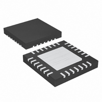
MAX1193ETI+ Maxim Integrated Products, MAX1193ETI+ Datasheet - Page 13

MAX1193ETI+
Manufacturer Part Number
MAX1193ETI+
Description
IC ADC 8BIT 45MSPS DUAL 28-TQFN
Manufacturer
Maxim Integrated Products
Datasheet
1.MAX1193ETI.pdf
(26 pages)
Specifications of MAX1193ETI+
Number Of Bits
8
Sampling Rate (per Second)
45M
Data Interface
Parallel
Number Of Converters
2
Voltage Supply Source
Single Supply
Operating Temperature
-40°C ~ 85°C
Mounting Type
Surface Mount
Package / Case
28-WFQFN Exposed Pad
Conversion Rate
45 MSPs
Resolution
8 bit
Snr
48.5 dB
Voltage Reference
1.024 V
Supply Voltage (max)
3.6 V
Supply Voltage (min)
2.7 V
Maximum Power Dissipation
1667 mW
Maximum Operating Temperature
+ 85 C
Mounting Style
SMD/SMT
Input Voltage
3 V
Minimum Operating Temperature
- 40 C
Lead Free Status / RoHS Status
Lead free / RoHS Compliant
Figure 1. Pipeline Architecture—Stage Blocks
Figure 2. MAX1193 Functional Diagram
INA+
INA-
PIN
23
24
25
26
27
—
FLASH
T/H
ADC
Ultra-Low-Power, 45Msps, Dual 8-Bit ADC
REFIN
NAME
REFIN
REFN
REFP
COM
REFN
COM
REFP
INA+
INB+
INA-
INB-
PD0
______________________________________________________________________________________
EP
T/H
STAGE 1
1.5 BITS
DAC
Power-Down Digital Input 0. See Table 3.
Reference Input. Internally pulled up to V
Common-Mode Voltage I/O. Bypass COM to GND with a 0.33µF capacitor.
Negative Reference I/O. Conversion range is ±(V
capacitor.
Positive Reference I/O. Conversion range is ±(V
capacitor.
Exposed Paddle. Internally connected to pin 3. Externally connect EP to GND.
DIGITAL ERROR CORRECTION
T/H
T/H
STAGE 2
+
∑
D0–D7
-
SYSTEM AND
REFERENCE
PIPELINE
PIPELINE
CIRCUITS
ADC
ADC
BIAS
A
B
x2
STAGE 7
/
/
DEC
DEC
MULTIPLEXER
The MAX1193 uses a seven-stage, fully differential,
pipelined architecture (Figure 1) that allows for high-
speed conversion while minimizing power consump-
tion. Samples taken at the inputs move progressively
through the pipeline stages every half-clock cycle.
Including the delay through the output latch, the total
clock-cycle latency is 5 clock cycles for channel A and
5.5 clock cycles for channel B.
At each stage, flash ADCs convert the held input volt-
ages into a digital code. The following digital-to-analog
converter (DAC) converts the digitized result back into
an analog voltage, which is then subtracted from the
originally held input signal. The resulting error signal is
then multiplied by two, and the product is passed along
to the next pipeline stage where the process is repeated
until the signal has been processed by all stages. Digital
error correction compensates for ADC comparator off-
sets in each pipeline stage and ensures no missing
codes. Figure 2 shows the MAX1193 functional diagram.
DD
.
FUNCTION
REFP
REFP
MAX1193
Pin Description (continued)
- V
- V
REFN
REFN
DRIVERS
OUTPUT
TIMING
). Bypass REFP to GND with a 0.33µF
CONTROL
). Bypass REFN to GND with a 0.33µF
POWER
Detailed Description
OV
V
GND
PD0
PD1
D0–D7
A/B
OGND
CLK
DD
DD
13


