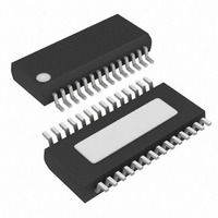
MAX1295ACEI+ Maxim Integrated Products, MAX1295ACEI+ Datasheet - Page 12

MAX1295ACEI+
Manufacturer Part Number
MAX1295ACEI+
Description
IC ADC 12BIT 265KSPS 28-QSOP
Manufacturer
Maxim Integrated Products
Datasheet
1.MAX1297BEEG.pdf
(19 pages)
Specifications of MAX1295ACEI+
Number Of Bits
12
Sampling Rate (per Second)
265k
Data Interface
Parallel
Number Of Converters
1
Power Dissipation (max)
762mW
Voltage Supply Source
Single Supply
Operating Temperature
0°C ~ 70°C
Mounting Type
Surface Mount
Package / Case
28-QSOP
Lead Free Status / RoHS Status
Lead free / RoHS Compliant
265ksps, +3V, 6-/2-Channel, 12-Bit ADCs
with +2.5V Reference and Parallel Interface
12
Figure 5. Conversion Timing Using External Acquisition Mode
Use external acquisition mode for precise control of the
sampling aperture and/or dependent control of acquisi-
tion and conversion times. The user controls acquisition
and start-of-conversion with two separate write pulses.
The first pulse, written with ACQMOD = 1, starts an
acquisition interval of indeterminate length. The second
write pulse, written with ACQMOD = 0 (all other bits in
control byte unchanged), terminates acquisition and
starts conversion on WR rising edge (Figure 5).
The address bits for the input multiplexer must have the
same values on the first and second write pulse.
Power-down mode bits (PD0, PD1) can assume new
values on the second write pulse (see Power-Down
Modes section). Changing other bits in the control byte
corrupts the conversion.
A standard interrupt signal INT is provided to allow the
MAX1295/MAX1297 to flag the µP when the conversion
has ended and a valid result is available. INT goes low
______________________________________________________________________________________
CS
D7–D0
INT
DOUT
WR
RD
HIGH-Z
HIGH-Z
t
DS
t
CSWS
ACQMOD = "1"
t
t
CS
WR
CONTROL
BYTE
Reading a Conversion
External Acquisition
t
t
CSHW
DH
t
ACQ
ACQMOD = "0"
CONTROL
BYTE
t
DH
t
CONV
when the conversion is complete and the output data is
ready (Figures 4 and 5). It returns high on the first read
cycle or if a new control byte is written.
The MAX1295/MAX1297 operate with either an internal
or an external clock. Control bits D6 and D7 select
either internal or external clock mode. The part retains
the last-requested clock mode if a power-down mode is
selected in the current input word. For both internal and
external clock mode, internal or external acquisition
can be used. At power-up, the MAX1295/MAX1297
enter the default external clock mode.
Select internal clock mode to release the µP from the
burden of running the SAR conversion clock. Bit D7 of
the control byte must be set to 1 and bit D6 must be set
to 0. The internal clock frequency is then selected,
resulting in a conversion time of 3.6µs. When using the
internal clock mode, tie the CLK pin either high or low
to prevent the pin from floating.
t
D0
t
INT1
DATA VALID
Selecting Clock Mode
Internal Clock Mode
HIGH-Z
HIGH-Z
t
TR


