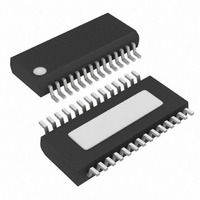
MAX1295ACEI+ Maxim Integrated Products, MAX1295ACEI+ Datasheet - Page 9

MAX1295ACEI+
Manufacturer Part Number
MAX1295ACEI+
Description
IC ADC 12BIT 265KSPS 28-QSOP
Manufacturer
Maxim Integrated Products
Datasheet
1.MAX1297BEEG.pdf
(19 pages)
Specifications of MAX1295ACEI+
Number Of Bits
12
Sampling Rate (per Second)
265k
Data Interface
Parallel
Number Of Converters
1
Power Dissipation (max)
762mW
Voltage Supply Source
Single Supply
Operating Temperature
0°C ~ 70°C
Mounting Type
Surface Mount
Package / Case
28-QSOP
Lead Free Status / RoHS Status
Lead free / RoHS Compliant
Table 1. Control-Byte Functional Description
Figure 3a. MAX1295 Simplified Input Structure
the analog inputs. This configuration is pseudo-differ-
ential in that only the signal at IN+ is sampled. The
return side (IN-) must remain stable within ±0.5 LSB
(±0.1 LSB for best performance) with respect to GND
during a conversion. To accomplish this, connect a
0.1µF capacitor from IN- (the selected input) to GND.
During the acquisition interval, the channel selected as
the positive input (IN+) charges capacitor C
D2, D1, D0
D7, D6
SINGLE-ENDED MODE: IN+ = CH0–CH5, IN- = COM
DIFFERENTIAL MODE: IN+ AND IN- SELECTED FROM PAIRS OF
BIT
COM
CH0
D5
D4
D3
CH1
CH2
CH3
CH4
CH5
V
REF
INPUT
MUX
with +2.5V Reference and Parallel Interface
ACQMOD
PD1, PD0
SGL/DIF
UNI/BIP
A2, A1, A0
12-BIT CAPACITIVE DAC
NAME
C
CH0/CH1 AND CH2/CH3, AND CH4/CH5
SWITCH
–
_______________________________________________________________________________________
12pF
C
HOLD
TRACK
SWITCH
+
265ksps, +3V, 6-/2-Channel, 12-Bit ADCs
T/H
PD1 and PD0 select the various clock and power-down modes.
R
800Ω
ACQMOD = 0: Internal Acquisition Mode
ACQMOD = 1: External Acquisition Mode
SGL/DIF = 0: Pseudo-Differential Analog Input Mode
SGL/DIF = 1: Single-Ended Analog Input Mode
In single-ended mode, input signals are referred to COM. In differential mode, the voltage difference
between two channels is measured (Tables 2, 4).
UNI/BIP = 0: Bipolar Mode
UNI/BIP = 1: Unipolar Mode
In unipolar mode, an analog input signal from 0V to V
signal can range from -V
Address bits A2, A1, A0 select which of the 6/2 (MAX1295/MAX1297) channels is to be converted
(Tables 2, 3).
IN
0
0
1
1
HOLD
ZERO
AT THE SAMPLING INSTANT,
THE MUX INPUT SWITCHES
FROM THE SELECTED IN+
CHANNEL TO THE SELECTED
IN- CHANNEL.
0
1
0
1
COMPARATOR
Full Power-Down Mode. Clock mode is unaffected.
Standby Power-Down Mode. Clock mode is unaffected.
Normal Operation Mode. Internal clock mode selected.
Normal Operation Mode. External clock mode selected.
HOLD
REF
. At the
/2 to +V
FUNCTIONAL DESCRIPTION
REF
end of the acquisition interval, the T/H switch opens,
retaining charge on C
at IN+.
The conversion interval begins with the input multiplex-
er switching C
negative input (IN-). This unbalances node ZERO at
the comparator’s positive input. The capacitive digital-
to-analog converter (DAC) adjusts during the remain-
Figure 3b. MAX1297 Simplified Input Structure
/2.
SINGLE-ENDED MODE: IN+ = CH0–CH1, IN- = COM
DIFFERENTIAL MODE: IN+ AND IN- SELECTED FROM PAIR
COM
CH0
CH1
V
REF
REF
INPUT
MUX
HOLD
12-BIT CAPACITIVE DAC
can be converted; in bipolar mode, the
C
CH0/CH1
SWITCH
–
12pF
C
from the positive input (IN+) to the
HOLD
TRACK
SWITCH
HOLD
+
T/H
R
800Ω
IN
as a sample of the signal
HOLD
ZERO
AT THE SAMPLING INSTANT,
THE MUX INPUT SWITCHES
FROM THE SELECTED IN+
CHANNEL TO THE SELECTED
IN- CHANNEL.
COMPARATOR
9


