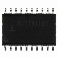
HI7191IBZ-T Intersil, HI7191IBZ-T Datasheet - Page 17

HI7191IBZ-T
Manufacturer Part Number
HI7191IBZ-T
Description
CONV A/D 24BIT SIGMA/DLTA 20SOIC
Manufacturer
Intersil
Datasheet
1.HI7191IBZ-T.pdf
(25 pages)
Specifications of HI7191IBZ-T
Number Of Bits
24
Data Interface
Serial, SPI™
Number Of Converters
1
Power Dissipation (max)
32.5mW
Voltage Supply Source
Analog and Digital, Dual ±
Operating Temperature
-40°C ~ 85°C
Mounting Type
Surface Mount
Package / Case
20-SOIC (0.300", 7.50mm Width)
Lead Free Status / RoHS Status
Lead free / RoHS Compliant
Other names
HI7191IBZ-TTR
Available stocks
Company
Part Number
Manufacturer
Quantity
Price
Company:
Part Number:
HI7191IBZ-T
Manufacturer:
Intersil
Quantity:
2 000
Programming the Serial Interface
It is useful to think of the HI7191 interface in terms of
communication cycles. Each communication cycle happens
in 2 phases. The first phase of every communication cycle
is the writing of an instruction byte. The second phase is
the data transfer as described by the instruction byte. It is
important to note that phase 2 of the communication cycle
can be a single byte or a multi-byte transfer of data. For
example, the 3-byte Data Output Register can be read
using one multi-byte communication cycle rather than three
single-byte communication cycles. It is up to the user to
maintain synchronism with respect to data transfers. If the
system processor “gets lost” the only way to recover is to
reset the HI7191. Figure 13 shows both a 2-wire and a
3-wire data transfer.
Several formats are available for reading from and writing to
the HI7191 registers in both the 2-wire and 3-wire protocols.
A portion of these formats is controlled by the CR<2:1> (BD
and MSB) bits which control the byte direction and bit order
of a data transfer respectively. These two bits can be written
in any combination but only the two most useful will be
discussed here.
The first combination is to reset both the BD and MSB bits
(BD = 0, MSB = 0). This sets up the interface for descending
byte order and MSB first format. When this combination is
used the user should always write the Instruction Register
such that the starting byte is the most significant byte
address. For example, read three bytes of DR starting with
the most significant byte. The first byte read will be the most
significant in MSB to LSB format. The next byte will be the
next least significant (recall descending byte order) again in
MSB to LSB order. The last byte will be the next lesser
significant byte in MSB to LSB order. The entire word was
read MSB to LSB format.
The second combination is to set both the BD and MSB bits
to 1. This sets up the interface for ascending byte order and
LSB first format. When this combination is used the user
should always write the Instruction Register such that the
starting byte is the least significant byte address. For
example, read three bytes of DR starting with the least
significant byte. The first byte read will be the least
significant in LSB to MSB format. The next byte will be the
next greater significant (recall ascending byte order) again in
LSB to MSB order. The last byte will be the next greater
OSC
SCLK
CS
1
17
29
FIGURE 12. SCLK OUTPUT IN SELF-CLOCKING MODE
33
37
HI7191
41
significant byte in LSB to MSB order. The entire word was
read MSB to LSB format.
After completion of each communication cycle, The HI7191
interface enters a standby mode while waiting to receive a
new instruction byte.
Instruction Byte Phase
The instruction byte phase initiates a data transfer
sequence. The processor writes an 8-bit byte (Instruction
Byte) to the Instruction Register. The instruction byte informs
the HI7191 about the Data transfer phase activities and
includes the following information:
• Read or Write cycle
• Number of Bytes to be transferred
• Which register and starting byte to be accessed
Data Transfer Phase
In the data transfer phase, data transfer takes place as set
by the Instruction Register contents. See Write Operation
and Read Operation sections for detailed descriptions.
SDIO
FIGURE 13A. 2-WIRE, 3-BYTE READ OR WRITE TRANSFER
SDIO
SDO
CS
CS
FIGURE 13B. 3-WIRE, 3-BYTE READ TRANSFER
45
INSTRUCTION
INSTRUCTION
INSTRUCTION
INSTRUCTION
CYCLE
CYCLE
BYTE
BYTE
89
BYTE 1
BYTE 1
DATA
DATA
DATA TRANSFER
DATA TRANSFER
BYTE 2
DATA
BYTE 2
DATA
121
BYTE 3
DATA
BYTE 3
DATA
125
June 1, 2006
FN4138.8


