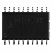
HI7191IBZ-T Intersil, HI7191IBZ-T Datasheet

HI7191IBZ-T
Specifications of HI7191IBZ-T
Available stocks
Related parts for HI7191IBZ-T
HI7191IBZ-T Summary of contents
Page 1
... HI7191IB HI7191IB - SOIC HI7191IBZ HI7191IBZ - SOIC (See Note) (Pb-free) HI7191IBZ-T HI7191IBZ - SOIC (See Note) Tape and Reel (Pb-free) HI7190EVAL Evaluation Kit NOTE: Intersil Pb-free plus anneal products employ special Pb-free material sets; molding compounds/die attach materials and 100% matte tin plate termination finish, which are RoHS compliant and compatible with both SnPb and Pb-free soldering operations ...
Page 2
Pinout HI7191 (PDIP, SOIC) TOP VIEW 1 20 SCLK SDO 2 19 SDIO DRDY 5 16 DGND RLO RHI ...
Page 3
Typical Application Schematic +5V INPUT + INPUT - REFERENCE -5V 0.1μF 3 HI7191 10MHz 17 16 OSC OSC 4.7μF 0.1μ INHI 11 V INLO +2.5V V RHI ...
Page 4
Absolute Maximum Ratings Supply Voltage AV to AGND ...
Page 5
Electrical Specifications AV DD PGIA Gain = 1, OSC PARAMETER Input Logic Current Input Capacitance DIGITAL OUTPUTS Output Logic High Voltage Output Logic Low Voltage Output Three-State Leakage Current Digital ...
Page 6
Timing Diagrams t CS SCLK SDIO CS SCLK SDIO SDO t ACC DRDY CS SCLK SDIO 1 6 HI7191 t PRE SCLK SCLKPW DSU SCLKPW t DHLD 1ST BIT FIGURE 1. DATA WRITE TO HI7191 1ST BIT ...
Page 7
Pin Descriptions 20 LEAD DIP, SOIC PIN NAME 1 SCLK Serial Interface Clock. Synchronizes serial data transfers. Data is input on the rising edge and output on the falling edge. 2 SDO Serial Data OUT. Serial data is read from ...
Page 8
TABLE 1. NOISE PERFORMANCE WITH INPUT CONNECTED TO ANALOG GROUND P-P NOISE HERTZ SNR ENOB GAIN = 1 10 132.3 21.7 25 129.5 21.2 30 127.7 20.9 50 126.3 20.7 60 125.6 20.6 100 122.4 20.0 250 107.7 17.6 500 ...
Page 9
Definitions Integral Non-Linearity, INL, is the maximum deviation of any digital code from a straight line passing through the endpoints of the transfer function. The endpoints of the transfer function are zero scale (a point 0.5 LSB below the first ...
Page 10
Motorola 6805/11 series SPI and Intel 8051 series SSR protocols. Data Integrity is always maintained at the HI7191 output port. This means that if a data read of conversion N is begun but not finished ...
Page 11
The output of the comparator is then fed back via a 1-bit DAC to the summing junction. The feedback loop forces the average of the fed back signal to be equal to the ...
Page 12
The HI7191 is designed to have a range of AV +1.8V < V < this range on the V pin will compromise ...
Page 13
NOT the absolute frequency. The error is seen when the user applies mid-scale (0V input, Bipolar mode). With this input, the expected digital output should be mid-scale (800000 ). Instead, there is a small h probability ...
Page 14
Scale Calibration Register, and 800000 (h) to the Negative Full Scale Calibration Register. This sets the offset correction factor to 0 and both the positive and negative gain slope factors to 1. The HI7191 offers several different modes of Self-Calibration ...
Page 15
System Offset/Internal Gain Calibration Mode Please note: System Offset/Internal Gain is only valid when operating in a gain of one. In addition, the offset and gain errors are not reduced as with the full system calibration. The System Offset/Internal Gain ...
Page 16
Normal operation in self-clocking mode is as follows (See Figure 12 sampled low on falling OSC SCLK transition output is delayed 29 OSC next rising OSC . SCLK transitions eight times and then stalls 1 high for 28 ...
Page 17
OSC 1 CS SCLK Programming the Serial Interface It is useful to think of the HI7191 interface in terms of communication cycles. Each communication cycle happens in 2 phases. The first phase of every communication cycle is the writing ...
Page 18
Instruction Register The Instruction Register is an 8-bit register which is used during a communications cycle for setting up read/write operations. MSB R/W MB1 MB0 FSC A3 R/W - Bit 7 of the Instruction Register determines ...
Page 19
Detailed Register Descriptions Data Output Register The Data Output Register contains 24 bits of converted data. This register is a read only register. BYTE 2 MSB D23 D22 D21 D20 D19 IR WRITE PHASE CS SCLK ...
Page 20
IR WRITE PHASE CS SCLK SDIO SDO THREE-STATE FIGURE 18. DATA READ CYCLE, 2-WIRE CONFIGURATION, SCLK IDLE LOW IR WRITE PHASE CS SCLK SDIO SDO THREE-STATE FIGURE ...
Page 21
G2 through G0 - Bits 7 through 5 select the gain of the input analog signal. The gain is accomplished through a programmable gain instrumentation amplifier that gains up incoming signals from This is achieved by using ...
Page 22
Offset Calibration Register The Offset Calibration Register is a 24-bit register containing the offset correction factor. This register is indeterminate on power-up but will contain a Self Calibration correction value after a RESET has been applied. BYTE 2 MSB 22 ...
Page 23
Die Characteristics DIE DIMENSIONS: 3550μm x 6340μm METALLIZATION: Type: AlSiCu Å Thickness: Metal 2, 16k Å Metal 1, 6k Metallization Mask Layout CS DRDY DGND HI7191 SUBSTRATE POTENTIAL (POWERED UP PASSIVATION: Type: Sandwich Å Thickness: ...
Page 24
Dual-In-Line Plastic Packages (PDIP INDEX N/2 AREA -B- -A- D BASE PLANE -C- SEATING PLANE 0.010 (0.25 NOTES: 1. Controlling Dimensions: INCH. In case of conflict between ...
Page 25
... Accordingly, the reader is cautioned to verify that data sheets are current before placing orders. Information furnished by Intersil is believed to be accurate and reliable. However, no responsibility is assumed by Intersil or its subsidiaries for its use; nor for any infringements of patents or other rights of third parties which may result from its use ...


