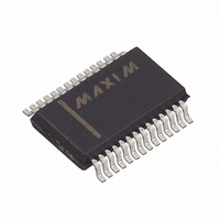
MAX1401EAI+ Maxim Integrated Products, MAX1401EAI+ Datasheet - Page 22

MAX1401EAI+
Manufacturer Part Number
MAX1401EAI+
Description
IC ADC 18BIT LP 28-SSOP
Manufacturer
Maxim Integrated Products
Datasheet
1.MAX1401EAI.pdf
(36 pages)
Specifications of MAX1401EAI+
Number Of Bits
18
Sampling Rate (per Second)
480
Data Interface
QSPI™, Serial, SPI™
Number Of Converters
1
Power Dissipation (max)
750µW
Voltage Supply Source
Analog and Digital
Operating Temperature
-40°C ~ 85°C
Mounting Type
Surface Mount
Package / Case
28-SSOP
Number Of Adc Inputs
5
Architecture
Delta-Sigma
Conversion Rate
4.8 KSPs
Resolution
18 bit
Input Type
Voltage
Interface Type
Serial
Voltage Reference
External
Supply Voltage (max)
3 V
Maximum Power Dissipation
21.45 mW
Maximum Operating Temperature
+ 85 C
Mounting Style
SMD/SMT
Input Signal Type
Pseudo-Differential, Differential
Minimum Operating Temperature
- 40 C
Lead Free Status / RoHS Status
Lead free / RoHS Compliant
+3V, 18-Bit, Low-Power, Multichannel,
Oversampling (Sigma-Delta) ADC
Table 11. Channel ID Tag Codes
A switching network provides selection between three
fully differential input channels or five pseudo-differen-
tial channels, using AIN6 as a shared common. The
switching network provides two additional fully differen-
tial input channels intended for system calibration,
which may be used as extra fully differential signal
channels. Table 12 shows the channel configurations
available for both operating modes.
Table 12. Input Channel Configuration in Fully Differential and Pseudo-Differential
Mode (SCAN = 0)
X = Don’t care
* This combination is available only in pseudo-differential mode when using the internal scanning logic.
** These combinations are only available in the calibration modes.
22
CID2
M1
______________________________________________________________________________________
0
0
0
0
0
0
1
0
0
0
0
1
0
0
0
0
1
1
1
1
CID1
M0
0
0
0
0
0
1
0
0
0
0
1
0
0
0
1
1
0
0
1
1
DIFF
CID0
0
0
0
0
X
X
X
1
1
1
X
X
0
1
0
1
0
1
0
1
Switching Network
A1
CHANNEL
AIN1–AIN6
AIN2–AIN6
AIN3–AIN6
AIN4–AIN6
AIN1–AIN2
AIN3–AIN4
AIN5–AIN6
0
0
1
1
X
X
X
0
0
1
X
X
Calibration
A0
0
1
0
1
X
X
X
0
1
0
X
X
To sample and convert the available input channels
sequentially, set the SCAN control bit in the global
setup register. The sequence is determined by DIFF
(fully differential or pseudo-differential) and by the
mode control bits M1 and M0 (Tables 8, 9, and 10).
With SCAN set, the part automatically sequences
through each available channel, transmitting a single
conversion result before proceeding to the next chan-
nel. The MAX1401 automatically allows sufficient time
for each conversion to fully settle, to ensure optimum
resolution before asserting the data-ready signal and
moving to the next available channel. The scan rate,
therefore, depends on the clock bit (CLK), the filter
control bits (FS1, FS0), and the modulator frequency
selection bits (MF1, MF0).
The input circuitry also provides two “burn-out” cur-
rents. These small currents may be used to test the
integrity of the selected transducer. They can be selec-
tively enabled or disabled by the BOUT bit in the global
setup register.
Differential
Differential
Pseudo-
MODE
Fully
HIGH INPUT
CALGAIN+**
CALGAIN+**
CALOFF+**
CALOFF+**
AIN5*
AIN2
AIN3
AIN4
AIN3
AIN5
AIN1
AIN1
Scanning (SCAN Mode)
Burn-Out Currents
LOW INPUT
CALGAIN-**
CALGAIN-**
CALOFF-**
CALOFF-**
AIN6*
AIN6
AIN6
AIN6
AIN6
AIN2
AIN4
AIN6


