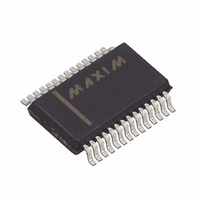
MAX1401EAI+ Maxim Integrated Products, MAX1401EAI+ Datasheet - Page 35

MAX1401EAI+
Manufacturer Part Number
MAX1401EAI+
Description
IC ADC 18BIT LP 28-SSOP
Manufacturer
Maxim Integrated Products
Datasheet
1.MAX1401EAI.pdf
(36 pages)
Specifications of MAX1401EAI+
Number Of Bits
18
Sampling Rate (per Second)
480
Data Interface
QSPI™, Serial, SPI™
Number Of Converters
1
Power Dissipation (max)
750µW
Voltage Supply Source
Analog and Digital
Operating Temperature
-40°C ~ 85°C
Mounting Type
Surface Mount
Package / Case
28-SSOP
Number Of Adc Inputs
5
Architecture
Delta-Sigma
Conversion Rate
4.8 KSPs
Resolution
18 bit
Input Type
Voltage
Interface Type
Serial
Voltage Reference
External
Supply Voltage (max)
3 V
Maximum Power Dissipation
21.45 mW
Maximum Operating Temperature
+ 85 C
Mounting Style
SMD/SMT
Input Signal Type
Pseudo-Differential, Differential
Minimum Operating Temperature
- 40 C
Lead Free Status / RoHS Status
Lead free / RoHS Compliant
For best performance, use printed circuit boards with
separate analog and digital ground planes. Wire-wrap
boards are not recommended.
Design the printed circuit board so the analog and digi-
tal sections are separated and confined to different
areas of the board. Join the digital and analog ground
planes at only one point. If the MAX1401 is the only
device requiring an AGND to DGND connection, then
the ground planes should be connected at the AGND
and DGND pins of the MAX1401. In systems where
multiple devices require AGND to DGND connections,
the connection should still be made at only one point.
Make the star ground as close to the MAX1401 as pos-
sible.
Avoid running digital lines under the device, because
these may couple noise onto the die. Run the analog
ground plane under the MAX1401 to minimize coupling
of digital noise. Make the power-supply lines to the
MAX1401 as wide as possible to provide low-imped-
ance paths and reduce the effects of glitches on the
power-supply line.
______________________________________________________________________________________
+3V, 18-Bit, Low-Power, Multichannel,
Grounding and Layout
Oversampling (Sigma-Delta) ADC
Shield fast switching signals, such as clocks, with digi-
tal ground to avoid radiating noise to other sections of
the board. Avoid running clock signals near the analog
inputs. Avoid crossover of digital and analog signals.
Traces on opposite sides of the board should run at
right angles to each other. This will reduce the effects
of feedthrough on the board. A microstrip technique is
best, but is not always possible with double-sided
boards. In this technique, the component side of the
board is dedicated to ground planes while signals are
placed on the solder side.
Good decoupling is important when using high-resolu-
tion ADCs. Decouple all analog supplies with 10µF tan-
talum capacitors in parallel with 0.1µF HF ceramic
capacitors to AGND. Place these components as close
to the device as possible to achieve the best decou-
pling.
See the MAX1403 evaluation kit manual for recom-
mended layout. The evaluation board package
includes a fully assembled and tested evaluation
board.
TRANSISTOR COUNT: 34,648
SUBSTRATE CONNECTED TO AGND
Chip Information
35


