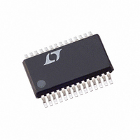
LTC2439-1IGN Linear Technology, LTC2439-1IGN Datasheet - Page 15

LTC2439-1IGN
Manufacturer Part Number
LTC2439-1IGN
Description
IC ADC 16BIT 16CH MCRPWR 28SSOP
Manufacturer
Linear Technology
Datasheet
1.LTC2439-1CGN.pdf
(28 pages)
Specifications of LTC2439-1IGN
Number Of Bits
16
Sampling Rate (per Second)
6.8
Data Interface
MICROWIRE™, Serial, SPI™
Number Of Converters
1
Power Dissipation (max)
1mW
Voltage Supply Source
Single Supply
Operating Temperature
-40°C ~ 85°C
Mounting Type
Surface Mount
Package / Case
28-SSOP (0.150", 3.95mm Width)
Lead Free Status / RoHS Status
Contains lead / RoHS non-compliant
Available stocks
Company
Part Number
Manufacturer
Quantity
Price
Part Number:
LTC2439-1IGN#TRPBF
Manufacturer:
LINEAR/凌特
Quantity:
20 000
APPLICATIO S I FOR ATIO
is seen while CS is LOW. The input data is then shifted in
via the SDI pin on the rising edge of SCK (including the
first rising edge) and the output data is shifted out of the
SDO pin on each falling edge of SCK. This enables
external circuitry to latch the output on the rising edge of
SCK. EOC can be latched on the first rising edge of SCK
and the last bit of the conversion result can be latched on
the 19th rising edge of SCK. On the 19th falling edge of
SCK, the device begins a new conversion. SDO goes HIGH
(EOC = 1) indicating a conversion is in progress.
At the conclusion of the data cycle, CS may remain LOW
and EOC monitored as an end-of-conversion interrupt.
Alternatively, CS may be driven HIGH setting SDO to Hi-Z.
As described above, CS may be pulled LOW at any time in
order to monitor the conversion status.
Typically, CS remains LOW during the data output state.
However, the data output state may be aborted by pulling
CS HIGH anytime between the first rising edge and the19th
falling edge of SCK, see Figure 7. On the rising edge of CS,
the device aborts the data output state and immediately
initiates a new conversion. If the device has not finished
loading the last input bit A0 of SDI by the time CS is pulled
HIGH, the address information is discarded and the previ-
(EXTERNAL)
SDO
SCK
SDI
CS
CONVERSION
Hi-Z
TEST EOC
SLEEP
(OPTIONAL)
TEST EOC
DON’T CARE
U
SLEEP
Hi-Z
U
BIT 18
(1)
EOC
BIT 17
(0)
(0)
W
Figure 6. External Serial Clock, Single Cycle Operation
EN
BIT 16
SIG
0.1V TO V
REFERENCE
ANALOG
INPUTS
VOLTAGE
U
SGL
1µF
BIT 15
2.7V TO 5.5V
MSB
CC
•
•
•
•
•
•
11
12
21
28
10
9
1
8
ODD/
SIGN
BIT 14
V
REF
REF
CH0
CH7
CH8
CH15
COM
CC
LTC2439-1
•
•
•
•
•
•
+
–
GND
SDO
SCK
SDI
A2
BIT 13
CS
F
ous address is kept. This is useful for aborting an invalid
conversion cycle or synchronizing the start of a conversion.
External Serial Clock, 3-Wire I/O
This timing mode utilizes a 3-wire serial I/O interface. The
conversion result is shifted out of the device by an exter-
nally generated serial clock (SCK) signal, see Figure 8. CS
may be permanently tied to ground, simplifying the user
interface or isolation barrier.
The external serial clock mode is selected at the end of the
power-on reset (POR) cycle. The POR cycle is concluded
typically 1ms after V
level applied to SCK at this time determines if SCK is
internal or external. SCK must be driven LOW prior to the
end of POR in order to enter the external serial clock timing
mode.
Since CS is tied LOW, the end-of-conversion (EOC) can be
continuously monitored at the SDO pin during the convert
and sleep states. EOC may be used as an interrupt to an
external controller indicating the conversion result is
ready. EOC = 1 while the conversion is in progress and
EOC = 0 once the conversion ends. On the falling edge of
EOC, the conversion result is loaded into an internal static
O
DATA OUTPUT
17
15
20
18
19
16
BIT 12
A1
4-WIRE
SPI INTERFACE
= EXTERNAL CLOCK SOURCE
= INTERNAL OSC/SIMULTANEOUS
50Hz/60Hz REJECTION
BIT 11
A0
CC
DON’T CARE
exceeds approximately 2V. The
BIT 6
LTC2439-1
BIT 0
LBS
CONVERSION
Hi-Z
15
TEST EOC
24391fa
24391 F05


