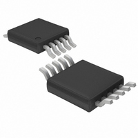
LTC2402CMS Linear Technology, LTC2402CMS Datasheet - Page 26

LTC2402CMS
Manufacturer Part Number
LTC2402CMS
Description
IC ADC 24BIT 2CH MICROPWR 10MSOP
Manufacturer
Linear Technology
Datasheet
1.LTC2401CMSPBF.pdf
(32 pages)
Specifications of LTC2402CMS
Number Of Bits
24
Sampling Rate (per Second)
7.5
Data Interface
MICROWIRE™, Serial, SPI™
Number Of Converters
2
Power Dissipation (max)
1mW
Voltage Supply Source
Single Supply
Operating Temperature
0°C ~ 70°C
Mounting Type
Surface Mount
Package / Case
10-TFSOP, 10-MSOP (0.118", 3.00mm Width)
Lead Free Status / RoHS Status
Contains lead / RoHS non-compliant
Available stocks
Company
Part Number
Manufacturer
Quantity
Price
Company:
Part Number:
LTC2402CMS
Manufacturer:
LT
Quantity:
10 000
Part Number:
LTC2402CMS
Manufacturer:
LINEAR/凌特
Quantity:
20 000
Part Number:
LTC2402CMS#PBF
Manufacturer:
LINEAR/凌特
Quantity:
20 000
APPLICATIO S I FOR ATIO
LTC2401/LTC2402
ANTIALIASING
One of the advantages delta-sigma ADCs offer over con-
ventional ADCs is on-chip digital filtering. Combined with
a large oversampling ratio, the LTC2401/LTC2402 signifi-
cantly simplify antialiasing filter requirements.
The digital filter provides very high rejection except at
integer multiples of the modulator sampling frequency
(f
256 • F
or 60Hz). The bandwidth of signals not rejected by the
digital filter is narrow ( 0.2%) compared to the bandwidth
of the frequencies rejected.
As a result of the oversampling ratio (256) and the digital
filter, minimal (if any) antialias filtering is required in front
of the LTC2401/LTC2402. If passive RC components are
placed in front of the LTC2401/LTC2402, the input dy-
namic current should be considered (see Input Current
section). In cases where large effective RC time constants
are used, an external buffer amplifier may be required to
minimize the effects of input dynamic current.
The modulator contained within the LTC2401/LTC2402
can handle large-signal level perturbations without satu-
rating. Signal levels up to 40% of V
analog modulator. These signals are limited by the input
ESD protection to 300mV below ground and 300mV above
V
26
CC
S
), see Figure 26. The modulator sampling frequency is
.
O
, where F
–100
–140
–120
–20
–40
–60
–80
0
0
Figure 26. Sinc
O
is the notch frequency (typically 50Hz
U
INPUT FREQUENCY
U
f
S
4
/2
Filter Rejection
REF
W
do not saturate the
24012 F26
f
S
U
Single Ended Half-Bridge Digitizer
with Reference and Ground Sensing
Sensors convert real world phenomena (temperature,
pressure, gas levels, etc.) into a voltage. Typically, this
voltage is generated by passing an excitation current
through the sensor. The wires connecting the sensor to
the ADC form parasitic resistors R
tion current also flows through parasitic resistors R
R
parasitic resistors leads to systematic offset and full-scale
errors.
In order to eliminate the errors associated with these
parasitic resistors, the LTC2401/LTC2402 include a full-
scale set input (FS
(ZS
current full-scale sense input. Errors due to parasitic
resistance R
removed by the FS
scale output of the ADC (data out = FFFFFF
P2
SET
, as shown in Figure 27. The voltage drop across these
). As shown in Figure 28, the FS
I
EXCITATION
Figure 27. Errors Due to Excitation Currents
Figure 28. Half-Bridge Digitizer with
Zero-Scale and Full-Scale Sense
I
P1
EXCITATION
R
R
V
V
P1
P2
B
A
in series with the half-bridge sensor are
I
I
I
SET
DC
DC
DC
R
R
R
P3
P4
P5
= 0
= 0
= 0
SET
input to the ADC. The absolute full-
R
R
2
3
5
6
P1
SENSOR
P2
) and a zero-scale set input
FS
V
ZS
GND
IN
SET
LTC2401
SET
+
–
+
–
V
V
V
CC
FULL-SCALE ERROR
OFFSET ERROR
1
+
–
SDO
SCK
CS
F
SENSOR OUTPUT
O
P1
9
8
7
10
and R
SET
24012 F03
3-WIRE
SPI INTERFACE
24012 F27
pin acts as a zero
HEX
P2
. The excita-
) will occur
P1
and


