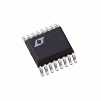
LTC2410CGN Linear Technology, LTC2410CGN Datasheet - Page 11

LTC2410CGN
Manufacturer Part Number
LTC2410CGN
Description
IC ADC 24BIT DIFF INP/REF 16SSOP
Manufacturer
Linear Technology
Datasheet
1.LTC2410CGNPBF.pdf
(48 pages)
Specifications of LTC2410CGN
Number Of Bits
24
Sampling Rate (per Second)
7.5
Data Interface
MICROWIRE™, Serial, SPI™
Number Of Converters
2
Power Dissipation (max)
1mW
Voltage Supply Source
Single Supply
Operating Temperature
0°C ~ 70°C
Mounting Type
Surface Mount
Package / Case
16-SSOP (0.150", 3.90mm Width)
Lead Free Status / RoHS Status
Contains lead / RoHS non-compliant
Other names
Q894257
Available stocks
Company
Part Number
Manufacturer
Quantity
Price
Part Number:
LTC2410CGN
Manufacturer:
LINEAR/凌特
Quantity:
20 000
Part Number:
LTC2410CGN#PBF
Manufacturer:
LINEAR/凌特
Quantity:
20 000
Part Number:
LTC2410CGN-1
Manufacturer:
LINEAR/凌特
Quantity:
20 000
FU CTIO AL BLOCK DIAGRA
TEST CIRCUITS
APPLICATIO S I FOR ATIO
CONVERTER OPERATION
Converter Operation Cycle
The LTC2410 is a low power, delta-sigma analog-to-
digital converter with an easy to use 3-wire serial interface
(see Figure 1). Its operation is made up of three states. The
converter operating cycle begins with the conversion,
followed by the low power sleep state and ends with the
data output (see Figure 2). The 3-wire interface consists
of serial data output (SDO), serial clock (SCK) and chip
select (CS).
Initially, the LTC2410 performs a conversion. Once the
conversion is complete, the device enters the sleep state.
While in this sleep state, power consumption is reduced by
an order of magnitude. The part remains in the sleep state
REF
REF
GND
V
IN
IN
CC
+
–
+
–
U
+
–
U
SDO
U
Hi-Z TO V
V
V
1.69k
– +
OL
OH
U
DAC
TO V
TO Hi-Z
OH
OH
C
LOAD
W
2410 TA03
= 20pF
Figure 1. Functional Block Diagram
U
W
as long as CS is HIGH. The conversion result is held
indefinitely in a static shift register while the converter is
in the sleep state.
ADC
Figure 2. LTC2410 State Transition Diagram
SDO
AUTOCALIBRATION
FALSE
DECIMATING FIR
AND CONTROL
Hi-Z TO V
V
V
OH
OL
V
TO Hi-Z
TO V
DATA OUTPUT
CC
CONVERT
CS = LOW
1.69k
SCK
SLEEP
C
OL
OL
AND
LOAD
TRUE
2410 TA04
= 20pF
2410 F02
OSCILLATOR
INTERFACE
INTERNAL
LTC2410
SERIAL
(INT/EXT)
11
F
SDO
SCK
CS
2410 FD
O


