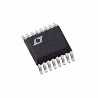
LTC2415-1CGN Linear Technology, LTC2415-1CGN Datasheet - Page 25

LTC2415-1CGN
Manufacturer Part Number
LTC2415-1CGN
Description
IC ADC 24BIT DIFFINPUT/REF16SSOP
Manufacturer
Linear Technology
Datasheet
1.LTC2415CGNPBF.pdf
(40 pages)
Specifications of LTC2415-1CGN
Number Of Bits
24
Sampling Rate (per Second)
13.75
Data Interface
MICROWIRE™, Serial, SPI™
Number Of Converters
2
Power Dissipation (max)
1mW
Voltage Supply Source
Single Supply
Operating Temperature
0°C ~ 70°C
Mounting Type
Surface Mount
Package / Case
16-SSOP (0.150", 3.90mm Width)
Lead Free Status / RoHS Status
Contains lead / RoHS non-compliant
Available stocks
Company
Part Number
Manufacturer
Quantity
Price
Company:
Part Number:
LTC2415-1CGN
Manufacturer:
LT
Quantity:
10 000
Part Number:
LTC2415-1CGN
Manufacturer:
LINEAR/凌特
Quantity:
20 000
Company:
Part Number:
LTC2415-1CGN#PBF
Manufacturer:
TI
Quantity:
120
Part Number:
LTC2415-1CGN#PBF
Manufacturer:
LINEAR/凌特
Quantity:
20 000
Part Number:
LTC2415-1CGN#TRPBF
Manufacturer:
LINEAR/凌特
Quantity:
20 000
APPLICATIO S I FOR ATIO
Timing Compatibility with the LTC2410/LTC2413
All timing modes described above are identical with re-
spect to the LTC2410/LTC2413 and LTC2415/LTC2415-1,
with one exception. The conversion time of the LTC2410
is 133ms while the conversion time of the LTC2415 is
Figure 17. CS Capacitance vs Supply Current
Figure 16. CS Capacitance vs Output Rate
Figure 15. CS Capacitance vs t
300
250
200
150
100
50
7
6
5
4
3
1
0
2
8
7
6
5
4
3
2
1
0
0
1
0
1
U
10
10
10
CAPACITANCE ON CS (pF)
CAPACITANCE ON CS (pF)
CAPACITANCE ON CS (pF)
V
V
CC
CC
V
CC
= 5V
= 3V
100
100
100
= 5V
U
1000
1000
1000
V
CC
V
= 5V
CC
10000
10000
10000
= 3V
V
CC
W
= 3V
2415 F15
2415 F16
2415 F17
100000
100000
100000
SAMPLE
U
66.6ms and the conversion time of the LTC2413 is 146ms,
while the LTC2415-1 is 73ms. In systems where the SDO
pin is monitored for the end-of-conversion signal (SDO
goes low once the conversion is complete) these two
devices can be interchanged. In cases where SDO is not
monitored, a wait state is inserted between conversions,
the duration of this wait state must be greater than 66.6ms
for the LTC2415, greater than 133ms for the LTC2410,
greater than 146ms for the LTC2413 and greater than
73ms for the LTC2415-1.
PRESERVING THE CONVERTER ACCURACY
The LTC2415/LTC2415-1 are designed to reduce as much
as possible conversion result sensitivity to device
decoupling, PCB layout, antialiasing circuits, line fre-
quency perturbations and so on. Nevertheless, in order to
preserve the extreme accuracy capability of this part,
some simple precautions are desirable.
Digital Signal Levels
The LTC2415/LTC2415-1 digital interface is easy to use.
Its digital inputs (F
operation) accept standard TTL/CMOS logic levels and the
internal hysteresis receivers can tolerate edge rates as slow
as 100 s. However, some considerations are required to
take advantage of the exceptional accuracy and low supply
current of this converter.
The digital output signals (SDO and SCK in Internal SCK
mode of operation) are less of a concern because they are
not generally active during conversion.
While a digital input signal is in the range 0.5V to
(V
current from the power supply. It should be noted that,
when any one of the digital input signals (F
in External SCK mode of operation) is within this range, the
LTC2415/LTC2415-1 power supply current may increase
even if the signal in question is at a valid logic level. For
micropower operation, it is recommended to drive all
digital input signals to full CMOS levels [V
V
During the conversion period, the undershoot and/or
overshoot of a fast digital signal connected to the LTC2415/
OH
CC
> (V
– 0.5V), the CMOS input receiver draws additional
CC
– 0.4V)].
LTC2415/LTC2415-1
O
, CS and SCK in External SCK mode of
O
IL
, CS and SCK
< 0.4V and
sn2415 24151fs
25


